Difference between revisions of "PIC16F877A PWM"
| Line 26: | Line 26: | ||
| + | =PWM Working= | ||
[[FILE:Pwm.png]]<br> | [[FILE:Pwm.png]]<br> | ||
| Line 45: | Line 46: | ||
Below diagram shows the PIC16f877a PWM block diagram and output signal generation. | Below diagram shows the PIC16f877a PWM block diagram and output signal generation. | ||
[[FILE:Pic16f877a_Pwm.png]]<br> | [[FILE:Pic16f877a_Pwm.png]]<br> | ||
| + | |||
| + | PIC uses the TIMER2 for generating the PWM signals. Lets relate the above concepts with the PIC registers. | ||
| + | <b>Period:</b><b>PR2</b> register is used to specify the PWM Period. The PWM period can be calculated using the following formula. | ||
| + | $$PWM Period = [(PR2) + 1] * 4 * TOSC * (TMR2 Prescale Value)$$ | ||
| + | |||
| + | <b>DutyCycle:</b>CCPR1L and CCP1CON<5:4> are used to specify the DutyCycle.The CCPR1L contains the eight MSbs and the CCP1CON<5:4> contains the two LSbs. | ||
=PIC16F877A PWM Registers= | =PIC16F877A PWM Registers= | ||
Revision as of 12:11, 14 May 2016
In this tutorial we are going to discuss the PWM module of PIC16F877A.
First we will see how to configure the PWM registers to generate signals of required PWM, At the end we will see how to use the ExploreEmdedded PWM library.
Contents
PIC16F877A PWM Module
PIC16F877A microcontroller has two independent CCP(Capture/Compare/PWM) modules, named as CCP1 and CCP2. Each CCP module has two 8-bit resistors(CCPxH,CCPxL) that can be use as:
- 16 bit Capture Register
- 16 bit Compare Register
- 10-bit PWM Register.
In this tutorial we will be discussing only the PWM part of CCP. PIC has 2PWM module with a resolution of 10-bits. The 8-Msb bits are stored in CCPRxL and remeining 2-bits in CCPxCON register. Below tables shows the PWM module of PIC.
| PWM Channel | Port Pin | Control Register | Duty Cycle Register | Period Register |
|---|---|---|---|---|
| PWM1 | PC.2 | CCP1CON | CCPR1L | PR2 |
| PWM2 | PC.1 | CCP2CON | CCPR2L | PR2 |
PWM Working
Before going to the PIC PWM module lets understand few terminologies:
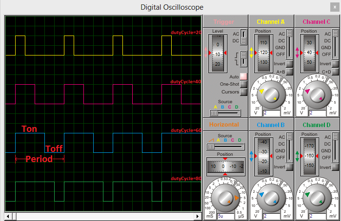
Ton: Time for which the signal is ON/HIGH.
Toff: Time for which the signal is OFF/LOW.
Period: The cycle time of the signal which is nothing but the sum of Ton and Toff period.
Period= Ton+Toff
Freq of Pwm signal;= 1/Period.
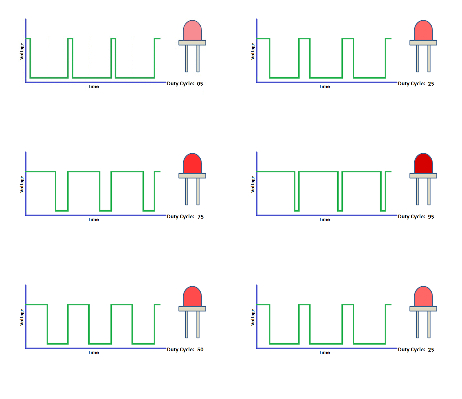
Duty Cycle: The percentage of time for which the PWM signal will be ON/HIGH. $$DutyCycle = (Ton/(Ton+Toff))*100 = (Ton/Period) * 100 $$
As shown in the above image the yellow signal is ON for 1 grid and the total period is of 5grids.
$$DutyCycle=(Ton/Period) * 100 = 1/5 * 100 = 20% $$
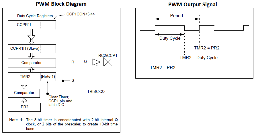
Below diagram shows the PIC16f877a PWM block diagram and output signal generation.

PIC uses the TIMER2 for generating the PWM signals. Lets relate the above concepts with the PIC registers. Period:PR2 register is used to specify the PWM Period. The PWM period can be calculated using the following formula. $$PWM Period = [(PR2) + 1] * 4 * TOSC * (TMR2 Prescale Value)$$
DutyCycle:CCPR1L and CCP1CON<5:4> are used to specify the DutyCycle.The CCPR1L contains the eight MSbs and the CCP1CON<5:4> contains the two LSbs.
PIC16F877A PWM Registers
The below table shows the registers associated with PIC16F877A PWM.
| Register | Description |
|---|---|
| CCPxCON | This register is used to Configure the CCP module for Capture/Compare/PWM opertaion. |
| CCPRxL | This register holds the 8-Msb bits of PWM, lower 2-bits will be part of CCPxCON register. |
| TMR2 | Free running counter which will be compared with CCPR1L and PR2 for generating the PWM output. |
Register Configuration
The below table shows the registers associated with LPC1768 PWM.
| CCPxCON | |||||||
| 7 | 6 | 5 | 4 | 3 | 2 | 1 | 0 |
| — | — | CCPxX | CCPxY | CCPxM3 | CCPxM2 | CCPxM1 | CCPxM0 |
CCPxX:CCPxY: PWM Least Significant bits
These bits are the two LSbs of the PWM duty cycle. The eight MSbs are found in CCPRxL.
CCPxM3:CCPxM0: CCPx Mode Select bits
0000 - Capture/Compare/PWM disabled (resets CCPx module)
0100 - Capture mode, every falling edge
0101 - Capture mode, every rising edge
0110 - Capture mode, every 4th rising edge
0111 - Capture mode, every 16th rising edge
1000 - Compare mode, set output on match (CCPxIF bit is set)
1001 - Compare mode, clear output on match (CCPxIF bit is set)
1010 - Compare mode, generate software interrupt on match (CCPxIF bit is set, CCPx pin is unaffected)
1011 - Compare mode, trigger special event (CCPxIF bit is set, CCPx pin is unaffected);
11xx - PWM mode
Steps to Configure PWM
- Configure the CCP1 module for PWM operation.
- Set the PWM period by writing to the PR2 register.
- Set the PWM duty cycle by writing to the CCPR1L register and CCP1CON<5:4> bits.
- Make the CCP1 pin an output by clearing the TRISC<2> bit.
- Set the TMR2 prescale value and enable Timer2 by writing to T2CON.
Example
Program to demonstrates the variable PWM signal generation.


