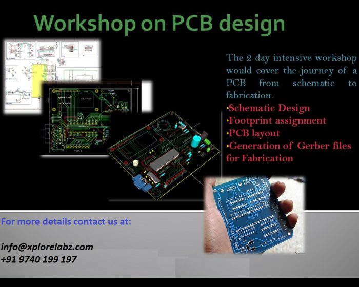
Workshop on PCB Design and Fabrication

The two day workshop would cover the following topics:
Need for PCB.
Introduction to KICAD.
A simple example: Schematic entry to PCB layout.
- Schematic Entry in detail:<br\>
- Creating custom components.
- Importing standard libraries.
- Tools for creating components.
- Generating Net list from schematic:<br\>
- Annotation schemes.
- Matching schematic symbols to footprints.
- Footprints:<br\>
- Component packages.
- Measurement units & standards.
- Library footprints.
- Importing footprints.
- Creating custom footprints.
- Tools for footprint generation.
- Board layout:<br\>
- Importing Net list.
- Footprint layout & form factor.
- Layers of design.
- Single layer, multilayer designs.
- Manual routing
- Custom Tracks & vias.
- Track width calculation.
- Auto Routing
- Outline routing tools.
- Generating custom routes.
- Gerber file generation:<br\>
- Finalizing the design.
- Gerber file format for different layers.
- Appending multiple boards.
- PCB Fabrication:<br\>
- Quick Presentation on PCB fabrication
- Checking FAB requirements.
