Difference between revisions of "PCB DesignWorkshop"
| Line 1: | Line 1: | ||
| − | + | {{box|type=blue_dark|text='''Workshop on PCB Design and Fabrication'''}} | |
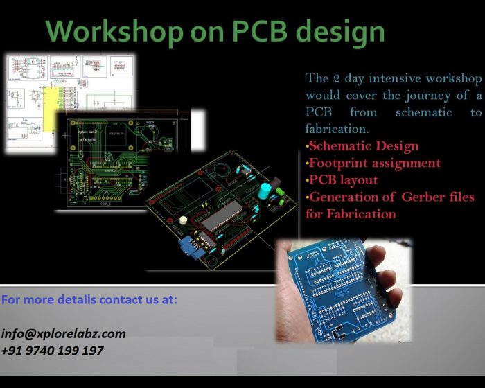
| − | [[File:PCBTemplate.png| | + | [[File:PCBTemplate.png|1080x560px]] |
| + | {{box|type=blue_light|text= | ||
| + | The two day workshop would cover the following topics: | ||
| + | *Schematic design using open source EDA tool KICAD. | ||
| + | *Net-list generation for the schematic. | ||
| + | *Assigning physical footprints to logical symbols in the schematic. | ||
| + | *Measuring footprint sizes with vernier calipers in both imperial and standard units. | ||
| + | *Creating custom components and footprints | ||
| + | *Importing net list to the PCB design suite | ||
| + | *Component layout as per design requirement | ||
| + | *Manual routing for single and double sided PCB boards. | ||
| + | *Auto routing using online router | ||
| + | *Generation of gerber files fabrication. | ||
| + | }} | ||
Revision as of 12:35, 4 December 2013
Workshop on PCB Design and Fabrication

The two day workshop would cover the following topics:
- Schematic design using open source EDA tool KICAD.
- Net-list generation for the schematic.
- Assigning physical footprints to logical symbols in the schematic.
- Measuring footprint sizes with vernier calipers in both imperial and standard units.
- Creating custom components and footprints
- Importing net list to the PCB design suite
- Component layout as per design requirement
- Manual routing for single and double sided PCB boards.
- Auto routing using online router
- Generation of gerber files fabrication.
