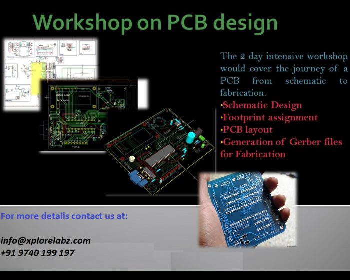
Workshop on PCB Design and Fabrication

The two day workshop would cover the following topics:
- Schematic design using open source EDA tool KICAD.
- Net-list generation for the schematic.
- Assigning physical footprints to logical symbols in the schematic.
- Measuring footprint sizes with vernier calipers in both imperial and standard units.
- Creating custom components and footprints
- Importing net list to the PCB design suite
- Component layout as per design requirement
- Manual routing for single and double sided PCB boards.
- Auto routing using online router
- Generation of gerber files fabrication.
