
Difference between revisions of "LPC1768: UART Programming"
| (114 intermediate revisions by 3 users not shown) | |||
| Line 1: | Line 1: | ||
[[category: LPC1768 Tutorials]] | [[category: LPC1768 Tutorials]] | ||
| − | |||
| − | |||
| − | |||
| − | |||
=Objective= | =Objective= | ||
| − | In this tutorial we are going to discuss the serial communication using UART. For more info on UART/RS232 check | + | In this tutorial we are going to discuss the serial communication using UART.<br> |
| + | For more info on UART/RS232 check [[A4.8051 Communication Protocols:UART, RS232|8051 tutorial]].<br> | ||
LPC1768 has four inbuilt USARTs. We are going to discuss only UART0. After this tutorial you should be able to extend it to remaining three UARTS.<br> | LPC1768 has four inbuilt USARTs. We are going to discuss only UART0. After this tutorial you should be able to extend it to remaining three UARTS.<br> | ||
| − | After understating the basics of LPC1768 UART module, We will discuss how to use the | + | After understating the basics of LPC1768 UART module, We will discuss how to use the ExploreEmbedded libraries to communicate with any of the UART devices.<br><br><br><br> |
| − | = | + | =UART module= |
| − | LPC1768 has | + | UART module and registers. |
| − | + | LPC1768 has 4-UARTs numbering 0-3, similarly the pins are also named as RXD0-RXD3 and TXD0-TXD3.As the LPC1768 pins are multiplexed for multiple functionalities, first they have to be configured as UART pins.<br> | |
| − | As LPC1768 | + | Below table shows the multiplexed UARTs pins.<br> |
| − | + | ||
| − | + | {| class="table table-striped table-hover table-condensed table-bordered" | |
| − | + | |-class="info" | |
| − | + | !Port Pin|| Pin Number || PINSEL_FUNC_0 || PINSEL_FUNC_1 ||PINSEL_FUNC_2 ||PINSEL_FUNC_3 | |
| − | {| class=" | + | |
| − | ! | + | |
|- | |- | ||
| − | + | |P0.02 || 98 || GPIO || <b>TXD0</b> || ADC0[7] || | |
| − | + | ||
| − | + | ||
| − | + | ||
| − | + | ||
| − | + | ||
| − | + | ||
| − | + | ||
| − | + | ||
| − | + | ||
| − | + | ||
| − | + | ||
| − | + | ||
| − | + | ||
| − | + | ||
| − | + | ||
| − | + | ||
| − | + | ||
| − | + | ||
| − | + | ||
| − | + | ||
| − | + | ||
| − | + | ||
| − | + | ||
| − | + | ||
| − | + | ||
| − | + | ||
| − | + | ||
|- | |- | ||
| − | | | + | |P0.03 || 99 || GPIO || <b>RXD0</b> || ADC0[6] || |
|- | |- | ||
| − | | | + | |P2_0 || 48 || GPIO || PWM1[1] || <b>TXD1</b> || |
|- | |- | ||
| − | | | + | |P2.1 || 49 || GPIO || PWM1[2] || <b>RXD1</b> || |
|- | |- | ||
| − | | | + | |P0.10 || 62 || GPIO || <b>TXD2</b> || SDA2|| MAT3[0] |
|- | |- | ||
| − | | | + | |P0.11 || 63 || GPIO || <b>RXD2</b> || SCL2|| MAT3[1] |
| − | | | + | |
| − | + | ||
| − | + | ||
| − | + | ||
| − | + | ||
| − | + | ||
| − | + | ||
| − | + | ||
| − | + | ||
| − | + | ||
| − | + | ||
| − | + | ||
| − | + | ||
|- | |- | ||
| − | | | + | |P0.0 || 82 || GPIO || CAN1_Rx|| <b>TXD3 </b>|| SDA1 |
|- | |- | ||
| − | | | + | |P0.1 || 85 || GPIO || CAN1_Tx|| <b>RXD3</b> || SCL1 |
|} | |} | ||
| + | <br><br><br><br> | ||
| − | + | =UART Registers = | |
| − | + | The below table shows the registers associated with LPC1768 UART.<br> | |
| − | + | {| class="table table-striped table-hover table-condensed table-bordered" | |
| − | + | |-class="info" | |
| − | + | !Register || Description | |
| − | The | + | |
| − | + | ||
| − | + | ||
| − | + | ||
| − | + | ||
| − | + | ||
| − | + | ||
| − | + | ||
| − | + | ||
| − | + | ||
| − | + | ||
| − | + | ||
| − | + | ||
| − | + | ||
| − | + | ||
| − | {| class=" | + | |
| − | ! | + | |
|- | |- | ||
| − | | | + | |RBR|| Contains the recently received Data |
|- | |- | ||
| − | | | + | |THR|| Contains the data to be transmitted |
| − | | | + | |- |
| − | + | |FCR|| FIFO Control Register | |
| − | + | ||
| − | + | ||
| − | + | ||
| − | + | ||
| − | + | ||
| − | + | ||
| − | + | ||
|- | |- | ||
| − | | | + | |LCR|| Controls the UART frame formatting(Number of Data Bits, Stop bits) |
|- | |- | ||
| − | | | + | |DLL|| Least Significant Byte of the UART baud rate generator value. |
|- | |- | ||
| + | |DLM|| Most Significant Byte of the UART baud rate generator value. | ||
|} | |} | ||
| + | <br><br> | ||
| − | + | =UART Register Configuration= | |
| − | + | Now lets see how to configure the individual registers for UART communication. | |
| − | == | + | ==FCR ( FIFO Control Register )== |
| − | {| class=" | + | LPC1768 has inbuilt 16byte FIFO for Receiver/Transmitter. Thus it can store 16-bytes of data received on UART without overwriting. If the data is not read before the Queue(FIFO) is filled then the new data will be lost and the OVERRUN error bit will be set. |
| − | + | {| class="table table-striped table-hover table-condensed table-bordered" | |
| + | |-class="info" | ||
| + | |FCR | ||
|- | |- | ||
| − | |31 | + | |31:8|| 7:6 || 5:4 || 3 || 2 || 1 || 0 |
|- | |- | ||
| − | | | + | |RESERVED|| RX TRIGGER|| RESERVED || DMA MODE || TX FIFO RESET || RX FIFO RESET || FIFO ENABLE |
|} | |} | ||
| − | '''Bit | + | '''Bit 0 – FIFO:'''<br> |
| − | This | + | This bit is used to enable/disable the FIFO for the data received/transmitted.<br> |
| − | + | 0--FIFO is Disabled.<br> | |
| + | 1--FIFO is Enabled for both Rx and Tx.<br> | ||
| + | |||
| + | '''Bit 1 – RX_FIFO:'''<br> | ||
| + | This is used to clear the 16-byte Rx FIFO.<br> | ||
| + | 0--No impact.<br> | ||
| + | 1--CLears the 16-byte Rx FIFO and the resets the FIFO pointer.<br> | ||
| + | '''Bit 2 – Tx_FIFO:'''<br> | ||
| + | This is used to clear the 16-byte Tx FIFO.<br> | ||
| + | 0--No impact.<br> | ||
| + | 1--Clears the 16-byte Tx FIFO and the resets the FIFO pointer.<br> | ||
| − | '''Bit | + | '''Bit 3 – DMA_MODE:'''<br> |
| − | + | This is used for Enabling/Disabling DMA mode.<br> | |
| + | 0--Disables the DMA.<br> | ||
| + | 1--Enables DMA only when the FIFO(bit-0) bit is SET.<br> | ||
| + | |||
| + | '''Bit 7:6 – Rx_TRIGGER:'''<br> | ||
| + | This bit is used to select the number of bytes of the receiver data to be written so as to enable the interrupt/DMA.<br> | ||
| + | 00-- Trigger level 0 (1 character or 0x01)<br> | ||
| + | 01-- Trigger level 1 (4 characters or 0x04)<br> | ||
| + | 10-- Trigger level 2 (8 characters or 0x08)<br> | ||
| + | 11-- Trigger level 3 (14 characters or 0x0E) | ||
| + | <br><br><br><br><br> | ||
| + | ==LCR ( Line Control Register )== | ||
| + | This register is used for defining the UART frame format ie. Number of Data bits, STOP bits etc. | ||
| + | {| class="table table-striped table-hover table-condensed table-bordered" | ||
| + | |-class="info" | ||
| + | |LCR | ||
| + | |- | ||
| + | |31:8|| 7 || 6 || 5:4 || 3 || 2 || 1:0 | ||
| + | |- | ||
| + | |Reserved|| DLAB || Break COntrol || Parity Select || Parity Enable || Stop Bit Select || Word Length Select | ||
| + | |} | ||
| + | |||
| + | '''Bit 1:0 – WLS : WordLenghtSelect'''<br> | ||
| + | These two bits are used to select the character length<br> | ||
| + | 00-- 5-bit character length<br> | ||
| + | 01-- 6-bit character length<br> | ||
| + | 10-- 7-bit character length<br> | ||
| + | 11-- 8-bit character length<br> | ||
| + | |||
| + | '''Bit 2 – Stop Bit Selection:'''<br> | ||
| + | This bit is used to select the number(1/2) of stop bits <br> | ||
| + | 0-- 1 Stop bit<br> | ||
| + | 1-- 2 Stop Bits<br> | ||
| − | '''Bit | + | '''Bit 3 – Parity Enable:'''<br> |
| − | This bit is | + | This bit is used to Enable or Disable the Parity generation and checking.<br> |
| + | 0-- Disable parity generation and checking.<br> | ||
| + | 1-- Enable parity generation and checking.<br> | ||
| + | |||
| + | '''Bit 5:4 – Parity Selection:'''<br> | ||
| + | These two bits will be used to select the type of parity.<br> | ||
| + | 00-- Odd parity. Number of 1s in the transmitted character and the attached parity bit will be odd.<br> | ||
| + | 01-- Even Parity. Number of 1s in the transmitted character and the attached parity bit will be even.<br> | ||
| + | 10-- Forced "1" stick parity.<br> | ||
| + | 11-- Forced "0" stick parity <br> | ||
| + | |||
| + | '''Bit 6 – Break Control'''<br> | ||
| + | 0-- Disable break transmission.<br> | ||
| + | 1-- Enable break transmission. Output pin UARTn TXD is forced to logic 0<br> | ||
| − | '''Bit | + | '''Bit 8 – DLAB: Divisor Latch Access Bit'''<br> |
| − | This bit is | + | This bit is used to enable the access to divisor latch.<br> |
| + | 0-- Disable access to divisor latch<br> | ||
| + | 0-- Enable access to divisor latch | ||
| + | <br><br><br><br><br> | ||
| − | == | + | ==LSR (Line Status Register)== |
| − | + | The is a read-only register that provides status information of the UART TX and RX blocks. | |
| + | {| class="table table-striped table-hover table-condensed table-bordered" | ||
| + | |-class="info" | ||
| + | |LSR | ||
| + | |- | ||
| + | |31:8 || 7 || 6 || 5 || 4 || 3 || 2 || 1|| 0 | ||
| + | |- | ||
| + | |Reserved || RXFE || TEMT || THRE || BI || FE || PE || OE || RDR | ||
| + | |} | ||
| − | + | '''Bit 0 – RDR: Receive Data Ready'''<br> | |
| + | This bit will be set when there is a received data in RBR register. This bit will be automatically cleared when RBR is empty.<br> | ||
| + | 0-- The UARTn receiver FIFO is empty.<br> | ||
| + | 1-- The UARTn receiver FIFO is not empty.<br> | ||
| + | |||
| + | '''Bit 1 – OE: Overrun Error'''<br> | ||
| + | The overrun error condition is set when the UART Rx FIFO is full and a new character is received. | ||
| + | In this case, the UARTn RBR FIFO will not be overwritten and the character in the UARTn RSR will be lost.<br> | ||
| + | 0-- No overrun<br> | ||
| + | 1-- Buffer over run<br> | ||
| − | + | '''Bit 2 – PE: Parity Error'''<br> | |
| − | + | This bit is set when the receiver detects a error in the Parity.<br> | |
| + | 0-- No Parity Error<br> | ||
| + | 1-- Parity Error<br> | ||
| + | |||
| + | '''Bit 3 – FE: Framing Error'''<br> | ||
| + | This bit is set when there is error in the STOP bit(LOGIC 0)<br> | ||
| + | 0-- No Framing Error<br> | ||
| + | 1-- Framing Error<br> | ||
| + | '''Bit 4 – BI: Break Interrupt'''<br> | ||
| + | This bit is set when the RXDn is held in the spacing state (all zeroes) for one full character transmission<br> | ||
| + | 0-- No Break interrupt<br> | ||
| + | 1-- Break Interrupt detected.<br> | ||
| + | '''Bit 5 – THRE: Transmitter Holding Register Empty'''<br> | ||
| + | THRE is set immediately upon detection of an empty THR. It is automatically cleared when the THR is written.<br> | ||
| + | 0-- THR register is Empty<br> | ||
| + | 1-- THR has valid data to be transmitted<br> | ||
| + | '''Bit 6 – TEMT: Transmitter Empty'''<br> | ||
| + | TEMT is set when both UnTHR and UnTSR are empty; TEMT is cleared when any of them contain valid data.<br> | ||
| + | 0-- THR and/or the TSR contains valid data.<br> | ||
| + | 1-- THR and the TSR are empty.<br> | ||
| + | '''Bit 7 – RXFE: Error in Rx FIFO'''<br> | ||
| + | This bit is set when the received data is affected by Framing Error/Parity Error/Break Error.<br> | ||
| + | 0-- RBR contains no UARTn RX errors.<br> | ||
| + | 1-- RBR contains at least one RX error.<br><br><br> | ||
| − | = | + | ==TER (Transmitter Enable register)== |
| − | + | This register is used to Enable/Disable the transmission | |
| + | {| class="table table-striped table-hover table-condensed table-bordered" | ||
| + | |-class="info" | ||
| + | |TER | ||
| + | |- | ||
| + | |31:8|| 7 || 6-0 | ||
| + | |- | ||
| + | |Reserved|| TXEN || Reserved | ||
| + | |} | ||
| + | |||
| + | |||
| + | '''Bit 7 – TXEN: Trsnamitter Enable<br> | ||
| + | When this bit is 1, the data written to the THR is output on the TXD pin.<br> | ||
| + | If this bit is cleared to 0 while a character is being sent, the transmission of that character is completed, but no further characters are sent until this bit is set again.<br> | ||
| + | In other words, a 0 in this bit blocks the transfer of characters. | ||
| + | *Note: By default this bit will be set after Reset.<br><br><br> | ||
| + | ==Baudrate Calculation== | ||
| + | LPC1768 generates the baud rate depending on the values of DLM,DLL.<br> | ||
| + | <b>Baudrate = PCLK/ (16 * ( 256 * DLM + DLL) * (1+ DivAddVal/MulVal))</b><br> | ||
| + | <b>Getting the PCLK value.</b><br> | ||
| + | PCLKSELx registers contains the PCLK info for all the clock dependent peripherals in which Bit6,Bit7 contains the Uart Clock(ie.UART_PCLK) information.<br> | ||
| + | The UART_PCLK and the actual Peripheral Clock(PCLK) is calculated as below.<br> | ||
| + | (Refer data sheet for more info) | ||
| + | {| class="table table-striped table-hover table-condensed table-bordered" | ||
| + | |-class="info" | ||
| + | |UART_PCLK || PCLK | ||
| + | |- | ||
| + | |0|| SystemFreq/4 | ||
| + | |- | ||
| + | |1|| SystemFreq | ||
| + | |- | ||
| + | |2|| SystemFreq/2 | ||
| + | |- | ||
| + | |3|| SystemFreq/8 | ||
| + | |} | ||
| + | |||
| + | |||
| + | DivAddVal/MulVal == 0 | ||
| + | |||
| + | Using the above parameters , DLL/DLM is calculated as below.<br> | ||
| + | <b>(256 * DLL + DLM) = PCLK / (16* Baudrate).</b><br><br><br> | ||
| − | |||
| − | |||
| − | |||
| − | |||
| − | |||
| − | |||
| − | |||
| − | |||
| − | |||
| − | |||
| − | |||
| + | =Steps for Configuring UART0= | ||
| + | Below are the steps for configuring the UART0. | ||
| + | #Step1: Configure the GPIO pin for UART0 function using PINSEL register. | ||
| + | #Step2: Configure the FCR for enabling the FIXO and Reste both the Rx/Tx FIFO. | ||
| + | #Step3: Configure LCR for 8-data bits, 1 Stop bit, Disable Parity and Enable DLAB. | ||
| + | #Step4: Get the PCLK from PCLKSELx register 7-6 bits. | ||
| + | #Step5: Calculate the DLM,DLL vaues for required baudrate from PCLK. | ||
| + | #Step6: Updtae the DLM,DLL with the calculated values. | ||
| + | #Step6: Finally clear DLAB to disable the access to DLM,DLL. | ||
| + | After this the UART will be ready to Transmit/Receive Data at the specified baudrate.<br> | ||
| + | <b>Code sniffet:</b> | ||
| + | <html> | ||
| + | <script src="https://gist.github.com/Amritach/35437ef514c0ad0f9089.js"></script> | ||
| + | </html> | ||
| + | <br><br> | ||
| + | =Steps for transmitting a char= | ||
| + | #Step1: Wait till the previous char is transmitted ie. till THRE becomes high. | ||
| + | #Step2: Load the new char to be transmitted into THR.<br> | ||
| + | <b>Code snippet</b> | ||
| + | <html> | ||
| + | <script src="https://gist.github.com/Amritach/50b91b48e5722b03ad4c.js"></script> | ||
| + | </html> | ||
| + | <br><br> | ||
| + | =Steps for Receiving a char= | ||
| + | #Step1: Wait till the a char is received ie. till RDR becomes high. | ||
| + | #Step2: Copy the received data from receive buffer(RBR).<br> | ||
| + | <b>Code snippet</b> | ||
| + | <html> | ||
| + | <script src="https://gist.github.com/Amritach/c6b329d11c5406347279.js"></script> | ||
| + | </html> | ||
=Code= | =Code= | ||
| − | |||
| − | |||
| − | |||
| − | |||
| − | |||
| − | |||
| − | |||
| − | |||
| − | |||
| − | |||
| − | |||
| − | |||
| − | |||
| − | |||
| + | ===Example 1=== | ||
| + | Below is the code for transmitting and receiving chars at 9600 baud<br> | ||
| + | <html> | ||
| + | <script src="https://gist.github.com/SaheblalBagwan/dfa8847f40f1cf14f20fae2bb2a6d83c.js"></script> | ||
| + | </html><br><br><br> | ||
| − | + | ===Using Explore Embedded Libraries=== | |
| − | + | In the above tutorial we discussed how to configure and use the inbuilt LPC1768 UART.<br> | |
| − | + | Now we will see how to use the ExploreEmbededd UART libraries to communicate on all the four UART channels.<br> | |
| − | + | For this you have to include the uart.c/uart.h files and associated gpio/stdutils files.<br> | |
| − | + | As LPC1768 has four inbuilt UART channels, the interfaces are suffixed with channel number as shown below.<br> | |
| − | + | UART0_Printf()<br> | |
| − | + | UART1_Printf()<br> | |
| + | UART2_Printf()<br> | ||
| + | UART3_Printf()<br> | ||
| − | + | #Note:Refer the uart.h file for more info. | |
| − | + | ||
| − | + | ||
| − | + | ||
| − | + | ||
| − | + | <html> | |
| + | <script src="https://gist.github.com/SaheblalBagwan/7db91d1895e3bfe9534c8f657af89a79.js"></script> | ||
| + | </html> | ||
| − | + | =Testing= | |
| − | + | ==Using the Terminal Software== | |
| + | After generating the hex/bin file, flash it to the controller. Now connect the LPC1768 to your system using a Usb to Serial converter. | ||
| − | + | [[File:Lpc1768SerialConnection.JPG|x400px]]<br><br> | |
| − | + | ||
| − | + | ||
| − | + | ||
| − | + | ||
| − | + | ||
| − | + | ||
| − | + | ||
| − | + | ||
| − | + | ||
| − | + | ||
| − | + | ||
| − | + | ||
| − | + | ||
| − | + | ||
| − | + | ||
| − | < | + | |
| + | Open the terminal software , select the COM port, set baud rate and hit the connect button. | ||
| + | <html> | ||
| + | <img src=https://www.exploreembedded.com/wiki/images/8/8f/TerminalSetUp.png class="img-responsive"> | ||
| + | </html><br><br> | ||
| + | ==Using The Keil Simulator== | ||
| + | Code can be tested on the Keil simulator as well. For this the target memory options needs to be set to default as shown below. | ||
| + | <html> | ||
| + | <img src=https://www.exploreembedded.com/wiki/images/d/d5/UartConfigOtpions.png class="img-responsive"> | ||
| + | </html> | ||
| − | |||
| − | |||
| − | |||
| − | |||
| − | |||
| − | |||
| − | |||
| − | |||
| − | |||
| − | |||
| − | |||
| − | + | Now Rebuild the project and Run the code using the Keil simulator as shown below. | |
| − | + | <html> | |
| − | + | <img src=https://www.exploreembedded.com/wiki/images/0/00/Lpc1768_Uart_Simulator.png class="img-responsive"> | |
| − | + | </html> | |
| − | + | <br><br> | |
| − | + | ||
| − | + | ||
| − | + | ||
| − | + | ||
| + | = Downloads= | ||
| + | Download the complete project folder from the below link: | ||
| + | https://codeload.github.com/ExploreEmbedded/Explore-Cortex-M3-LPC1768-Stick-DVB-14001/zip/master<br><br><br><br> | ||
| − | + | Have a opinion, suggestion , question or feedback about the article let it out here! | |
| − | + | ||
| − | + | ||
| − | + | ||
| − | + | ||
| − | + | ||
| − | + | ||
| − | + | ||
| − | + | ||
| − | + | ||
| − | + | ||
| − | + | ||
| − | + | ||
| − | + | ||
| − | + | ||
| − | + | ||
| − | + | ||
| − | + | ||
| − | + | ||
| − | + | ||
| − | + | ||
| − | + | ||
| − | + | ||
| − | + | ||
| − | + | ||
| − | + | ||
{{DISQUS}} | {{DISQUS}} | ||
Latest revision as of 11:59, 27 July 2016
Contents
Objective
In this tutorial we are going to discuss the serial communication using UART.
For more info on UART/RS232 check 8051 tutorial.
LPC1768 has four inbuilt USARTs. We are going to discuss only UART0. After this tutorial you should be able to extend it to remaining three UARTS.
After understating the basics of LPC1768 UART module, We will discuss how to use the ExploreEmbedded libraries to communicate with any of the UART devices.
UART module
UART module and registers.
LPC1768 has 4-UARTs numbering 0-3, similarly the pins are also named as RXD0-RXD3 and TXD0-TXD3.As the LPC1768 pins are multiplexed for multiple functionalities, first they have to be configured as UART pins.
Below table shows the multiplexed UARTs pins.
| Port Pin | Pin Number | PINSEL_FUNC_0 | PINSEL_FUNC_1 | PINSEL_FUNC_2 | PINSEL_FUNC_3 |
|---|---|---|---|---|---|
| P0.02 | 98 | GPIO | TXD0 | ADC0[7] | |
| P0.03 | 99 | GPIO | RXD0 | ADC0[6] | |
| P2_0 | 48 | GPIO | PWM1[1] | TXD1 | |
| P2.1 | 49 | GPIO | PWM1[2] | RXD1 | |
| P0.10 | 62 | GPIO | TXD2 | SDA2 | MAT3[0] |
| P0.11 | 63 | GPIO | RXD2 | SCL2 | MAT3[1] |
| P0.0 | 82 | GPIO | CAN1_Rx | TXD3 | SDA1 |
| P0.1 | 85 | GPIO | CAN1_Tx | RXD3 | SCL1 |
UART Registers
The below table shows the registers associated with LPC1768 UART.
| Register | Description |
|---|---|
| RBR | Contains the recently received Data |
| THR | Contains the data to be transmitted |
| FCR | FIFO Control Register |
| LCR | Controls the UART frame formatting(Number of Data Bits, Stop bits) |
| DLL | Least Significant Byte of the UART baud rate generator value. |
| DLM | Most Significant Byte of the UART baud rate generator value. |
UART Register Configuration
Now lets see how to configure the individual registers for UART communication.
FCR ( FIFO Control Register )
LPC1768 has inbuilt 16byte FIFO for Receiver/Transmitter. Thus it can store 16-bytes of data received on UART without overwriting. If the data is not read before the Queue(FIFO) is filled then the new data will be lost and the OVERRUN error bit will be set.
| FCR | ||||||
| 31:8 | 7:6 | 5:4 | 3 | 2 | 1 | 0 |
| RESERVED | RX TRIGGER | RESERVED | DMA MODE | TX FIFO RESET | RX FIFO RESET | FIFO ENABLE |
Bit 0 – FIFO:
This bit is used to enable/disable the FIFO for the data received/transmitted.
0--FIFO is Disabled.
1--FIFO is Enabled for both Rx and Tx.
Bit 1 – RX_FIFO:
This is used to clear the 16-byte Rx FIFO.
0--No impact.
1--CLears the 16-byte Rx FIFO and the resets the FIFO pointer.
Bit 2 – Tx_FIFO:
This is used to clear the 16-byte Tx FIFO.
0--No impact.
1--Clears the 16-byte Tx FIFO and the resets the FIFO pointer.
Bit 3 – DMA_MODE:
This is used for Enabling/Disabling DMA mode.
0--Disables the DMA.
1--Enables DMA only when the FIFO(bit-0) bit is SET.
Bit 7:6 – Rx_TRIGGER:
This bit is used to select the number of bytes of the receiver data to be written so as to enable the interrupt/DMA.
00-- Trigger level 0 (1 character or 0x01)
01-- Trigger level 1 (4 characters or 0x04)
10-- Trigger level 2 (8 characters or 0x08)
11-- Trigger level 3 (14 characters or 0x0E)
LCR ( Line Control Register )
This register is used for defining the UART frame format ie. Number of Data bits, STOP bits etc.
| LCR | ||||||
| 31:8 | 7 | 6 | 5:4 | 3 | 2 | 1:0 |
| Reserved | DLAB | Break COntrol | Parity Select | Parity Enable | Stop Bit Select | Word Length Select |
Bit 1:0 – WLS : WordLenghtSelect
These two bits are used to select the character length
00-- 5-bit character length
01-- 6-bit character length
10-- 7-bit character length
11-- 8-bit character length
Bit 2 – Stop Bit Selection:
This bit is used to select the number(1/2) of stop bits
0-- 1 Stop bit
1-- 2 Stop Bits
Bit 3 – Parity Enable:
This bit is used to Enable or Disable the Parity generation and checking.
0-- Disable parity generation and checking.
1-- Enable parity generation and checking.
Bit 5:4 – Parity Selection:
These two bits will be used to select the type of parity.
00-- Odd parity. Number of 1s in the transmitted character and the attached parity bit will be odd.
01-- Even Parity. Number of 1s in the transmitted character and the attached parity bit will be even.
10-- Forced "1" stick parity.
11-- Forced "0" stick parity
Bit 6 – Break Control
0-- Disable break transmission.
1-- Enable break transmission. Output pin UARTn TXD is forced to logic 0
Bit 8 – DLAB: Divisor Latch Access Bit
This bit is used to enable the access to divisor latch.
0-- Disable access to divisor latch
0-- Enable access to divisor latch
LSR (Line Status Register)
The is a read-only register that provides status information of the UART TX and RX blocks.
| LSR | ||||||||
| 31:8 | 7 | 6 | 5 | 4 | 3 | 2 | 1 | 0 |
| Reserved | RXFE | TEMT | THRE | BI | FE | PE | OE | RDR |
Bit 0 – RDR: Receive Data Ready
This bit will be set when there is a received data in RBR register. This bit will be automatically cleared when RBR is empty.
0-- The UARTn receiver FIFO is empty.
1-- The UARTn receiver FIFO is not empty.
Bit 1 – OE: Overrun Error
The overrun error condition is set when the UART Rx FIFO is full and a new character is received.
In this case, the UARTn RBR FIFO will not be overwritten and the character in the UARTn RSR will be lost.
0-- No overrun
1-- Buffer over run
Bit 2 – PE: Parity Error
This bit is set when the receiver detects a error in the Parity.
0-- No Parity Error
1-- Parity Error
Bit 3 – FE: Framing Error
This bit is set when there is error in the STOP bit(LOGIC 0)
0-- No Framing Error
1-- Framing Error
Bit 4 – BI: Break Interrupt
This bit is set when the RXDn is held in the spacing state (all zeroes) for one full character transmission
0-- No Break interrupt
1-- Break Interrupt detected.
Bit 5 – THRE: Transmitter Holding Register Empty
THRE is set immediately upon detection of an empty THR. It is automatically cleared when the THR is written.
0-- THR register is Empty
1-- THR has valid data to be transmitted
Bit 6 – TEMT: Transmitter Empty
TEMT is set when both UnTHR and UnTSR are empty; TEMT is cleared when any of them contain valid data.
0-- THR and/or the TSR contains valid data.
1-- THR and the TSR are empty.
Bit 7 – RXFE: Error in Rx FIFO
This bit is set when the received data is affected by Framing Error/Parity Error/Break Error.
0-- RBR contains no UARTn RX errors.
1-- RBR contains at least one RX error.
TER (Transmitter Enable register)
This register is used to Enable/Disable the transmission
| TER | ||
| 31:8 | 7 | 6-0 |
| Reserved | TXEN | Reserved |
Bit 7 – TXEN: Trsnamitter Enable
When this bit is 1, the data written to the THR is output on the TXD pin.
If this bit is cleared to 0 while a character is being sent, the transmission of that character is completed, but no further characters are sent until this bit is set again.
In other words, a 0 in this bit blocks the transfer of characters.
- Note: By default this bit will be set after Reset.
Baudrate Calculation
LPC1768 generates the baud rate depending on the values of DLM,DLL.
Baudrate = PCLK/ (16 * ( 256 * DLM + DLL) * (1+ DivAddVal/MulVal))
Getting the PCLK value.
PCLKSELx registers contains the PCLK info for all the clock dependent peripherals in which Bit6,Bit7 contains the Uart Clock(ie.UART_PCLK) information.
The UART_PCLK and the actual Peripheral Clock(PCLK) is calculated as below.
(Refer data sheet for more info)
| UART_PCLK | PCLK |
| 0 | SystemFreq/4 |
| 1 | SystemFreq |
| 2 | SystemFreq/2 |
| 3 | SystemFreq/8 |
DivAddVal/MulVal == 0
Using the above parameters , DLL/DLM is calculated as below.
(256 * DLL + DLM) = PCLK / (16* Baudrate).
Steps for Configuring UART0
Below are the steps for configuring the UART0.
- Step1: Configure the GPIO pin for UART0 function using PINSEL register.
- Step2: Configure the FCR for enabling the FIXO and Reste both the Rx/Tx FIFO.
- Step3: Configure LCR for 8-data bits, 1 Stop bit, Disable Parity and Enable DLAB.
- Step4: Get the PCLK from PCLKSELx register 7-6 bits.
- Step5: Calculate the DLM,DLL vaues for required baudrate from PCLK.
- Step6: Updtae the DLM,DLL with the calculated values.
- Step6: Finally clear DLAB to disable the access to DLM,DLL.
After this the UART will be ready to Transmit/Receive Data at the specified baudrate.
Code sniffet:
Steps for transmitting a char
- Step1: Wait till the previous char is transmitted ie. till THRE becomes high.
- Step2: Load the new char to be transmitted into THR.
Code snippet
Steps for Receiving a char
- Step1: Wait till the a char is received ie. till RDR becomes high.
- Step2: Copy the received data from receive buffer(RBR).
Code snippet
Code
Example 1
Below is the code for transmitting and receiving chars at 9600 baud
Using Explore Embedded Libraries
In the above tutorial we discussed how to configure and use the inbuilt LPC1768 UART.
Now we will see how to use the ExploreEmbededd UART libraries to communicate on all the four UART channels.
For this you have to include the uart.c/uart.h files and associated gpio/stdutils files.
As LPC1768 has four inbuilt UART channels, the interfaces are suffixed with channel number as shown below.
UART0_Printf()
UART1_Printf()
UART2_Printf()
UART3_Printf()
- Note:Refer the uart.h file for more info.
Testing
Using the Terminal Software
After generating the hex/bin file, flash it to the controller. Now connect the LPC1768 to your system using a Usb to Serial converter.

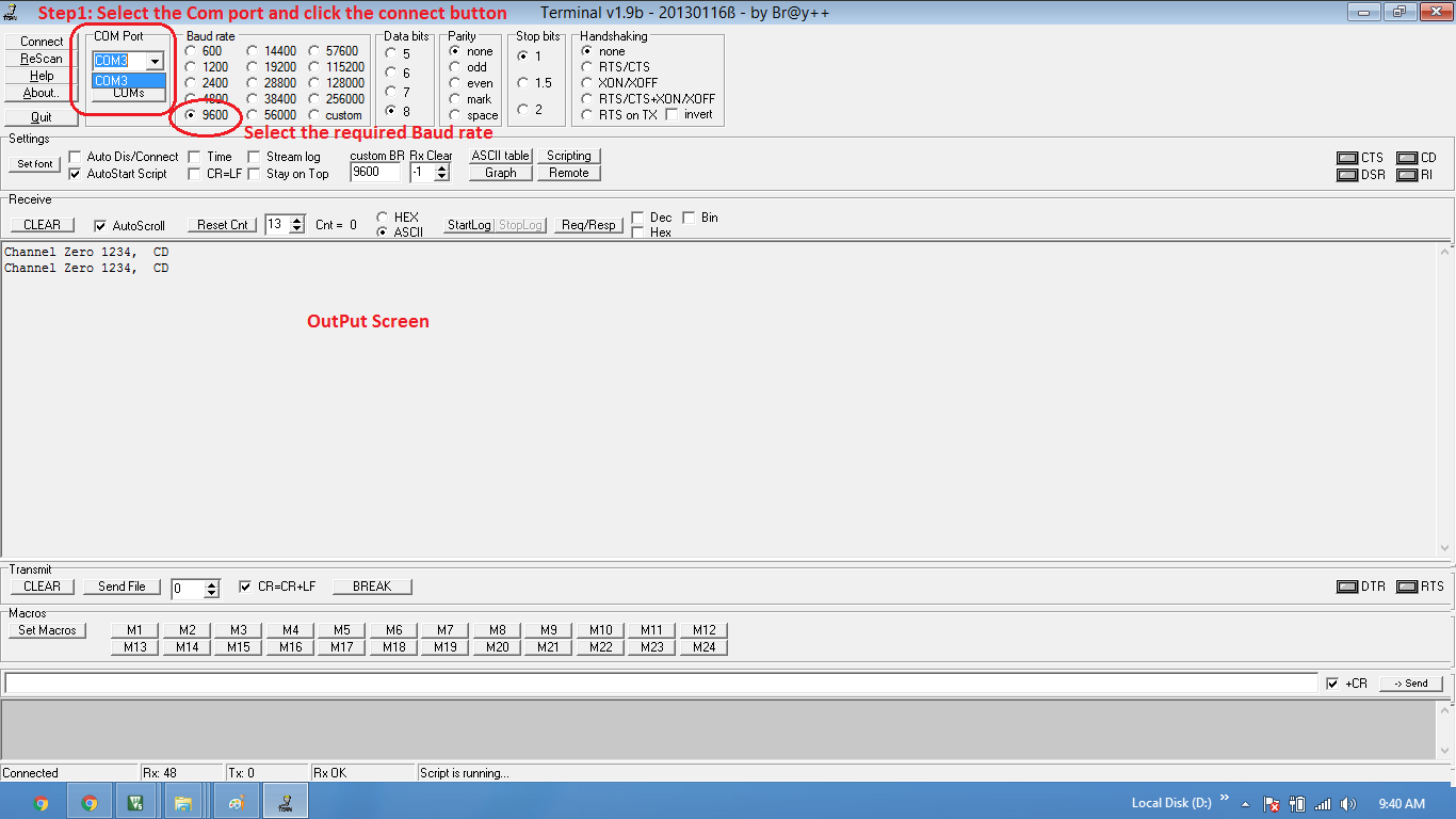
Open the terminal software , select the COM port, set baud rate and hit the connect button.
Using The Keil Simulator
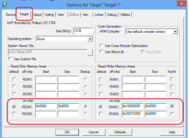
Code can be tested on the Keil simulator as well. For this the target memory options needs to be set to default as shown below.
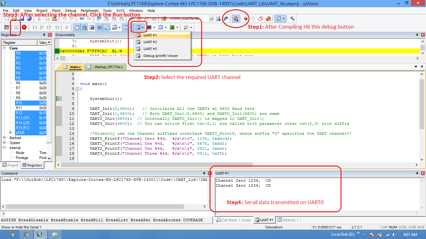
Now Rebuild the project and Run the code using the Keil simulator as shown below.
Downloads
Download the complete project folder from the below link:
https://codeload.github.com/ExploreEmbedded/Explore-Cortex-M3-LPC1768-Stick-DVB-14001/zip/master
Have a opinion, suggestion , question or feedback about the article let it out here!