
Difference between revisions of "LPC1768: Lcd 4bit"
(Created page with "category: LPC1768 Tutorials =Objective= This is first example on LPC1768 where we start with blinking the LEDs. In this tutorials we are going to discuss how to configur...") |
|||
| (88 intermediate revisions by 6 users not shown) | |||
| Line 1: | Line 1: | ||
[[category: LPC1768 Tutorials]] | [[category: LPC1768 Tutorials]] | ||
| + | In this tutorial we are going to see how to interface a 2x16 LCD with LPC1768 in 4-bit mode. | ||
| + | As per the name the 2x16 has 2 lines with 16 chars on each lines. It supports all the ascii chars and is basically used for displaying the alpha numeric characters. Here each character is displayed in a matrix of 5x7 pixels. | ||
| + | Apart from alpha numeric chars it also provides the provision to display the custom characters by creating the pattern. | ||
| + | Scope of this tutorial is to show how to display the alpha numeric chars on LCD, Generating and displaying the custom chars will be discussed in subsequent tutorials. | ||
| − | |||
| − | |||
| − | |||
| − | |||
| − | = | + | =LCD UNIT= |
| − | + | Let us look at a pin diagram of a commercially available LCD like '''JHD162''' which uses a '''HD44780''' controller and then describe its operation. | |
| − | + | [[FILE:Pic16f877aLcdInterface.png]] | |
| − | + | ||
| − | + | ||
| − | + | {| class="table table-striped table-hover table-condensed table-bordered" | |
| − | + | |-class="info" | |
| − | + | | Pin Number || Symbol || Pin Function | |
| − | + | ||
| − | + | ||
| − | + | ||
| − | + | ||
|- | |- | ||
| − | | | + | |1 || VSS ||Ground |
|- | |- | ||
| − | | | + | | 2|| VCC || +5v |
|- | |- | ||
| − | | | + | | 3 || VEE || Contrast adjustment (VO) |
|- | |- | ||
| − | | | + | | 4 || RS || Register Select. 0:Command, 1: Data |
| − | | | + | |
| − | + | ||
| − | + | ||
| − | + | ||
| − | + | ||
| − | + | ||
| − | + | ||
|- | |- | ||
| − | | | + | | 5 || R/W || Read/Write, R/W=0: Write & R/W=1: Read |
|- | |- | ||
| − | | | + | | 6|| EN || Enable. Falling edge triggered |
| − | | | + | |
| − | + | ||
| − | + | ||
| − | + | ||
| − | + | ||
| − | + | ||
| − | + | ||
|- | |- | ||
| − | |0|| | + | | 7 || D0 || Data Bit 0 (Not used in 4-bit operation) |
| + | |- | ||
| + | | 8 || D1 || Data Bit 1 (Not used in 4-bit operation) | ||
| + | |- | ||
| + | | 9 || D2 || Data Bit 2 (Not used in 4-bit operation) | ||
|- | |- | ||
| − | | | + | | 10 || D3 || Data Bit 3 (Not used in 4-bit operation) |
| − | + | ||
| − | + | ||
| − | + | ||
| − | + | ||
| − | + | ||
| − | + | ||
| − | + | ||
|- | |- | ||
| − | | | + | | 11 || D4 || Data Bit 4 |
| + | |- | ||
| + | | 12 || D5 || Data Bit 5 | ||
| + | |- | ||
| + | | 13 || D6 || Data Bit 6 | ||
| + | |- | ||
| + | | 14 || D7 || Data Bit 7/Busy Flag | ||
|- | |- | ||
| − | | | + | | 15 || A/LED+ || Back-light Anode(+) |
| − | + | ||
| − | + | ||
| − | + | ||
| − | + | ||
| − | + | ||
| − | + | ||
| − | + | ||
| − | |- | + | |
| − | + | ||
|- | |- | ||
| − | | | + | | 16 || K/LED- || Back-Light Cathode(-) |
|} | |} | ||
| + | <br><br> | ||
| + | Apart from the voltage supply connections the important pins from the programming perspective are the data lines(8-bit Data bus), Register select, Read/Write and Enable pin.<br><br> | ||
| + | <b>Data Bus:</b> As shown in the above figure and table, an alpha numeric lcd has a 8-bit data bus referenced as D0-D7. | ||
| + | As it is a 8-bit data bus, we can send the data/cmd to LCD in bytes. It also provides the provision to send the the data/cmd in chunks of 4-bit, which is used when there are limited number of GPIO lines on the microcontroller.<br><br> | ||
| + | <b>Register Select(RS):</b> The LCD has two register namely a Data register and Command register. Any data that needs to be displayed on the LCD has to be written to the data register of LCD. Command can be issued to LCD by writing it to Command register of LCD. | ||
| + | This signal is used to differentiate the data/cmd received by the LCD.<br> | ||
| + | If the RS signal is <b>LOW</b> then the LCD interprets the 8-bit info as <b>Command</b> and writes it <b>Command register</b> and performs the action as per the command.<br> | ||
| + | If the RS signal is <b>HIGH</b> then the LCD interprets the 8-bit info as <b>data</b> and copies it to <b>data register</b>. After that the LCD decodes the data for generating the 5x7 pattern and finally displays on the LCD.<br><br> | ||
| + | <b>Read/Write(RW):</b> This signal is used to write the data/cmd to LCD and reads the busy flag of LCD. | ||
| + | For write operation the RW should be <b>LOW</b> and for read operation the R/W should be <b>HIGH</b>.<br><br> | ||
| + | <b>Enable(EN):</b> This pin is used to send the enable trigger to LCD. | ||
| + | After sending the data/cmd, Selecting the data/cmd register, Selecting the Write operation. A HIGH-to-LOW pulse has to be send on this enable pin which will latch the info into the LCD register and triggers the LCD to act accordingly. | ||
| + | <br/> | ||
| + | <br/> | ||
| − | + | =Hardware Connections= | |
| − | + | [[File:LCD 4Bit.jpg|680px]] | |
| − | + | ||
| − | + | ||
| − | + | ||
| − | + | ||
| − | + | ||
| − | + | ||
| − | + | ||
| − | + | ||
| − | + | ||
| − | + | ||
| − | + | ||
=Schematic= | =Schematic= | ||
| + | Below schematic shows the minimum connection required for interfacing the LCD with the microcontroller.<br> | ||
| + | As we are interfacing the LCD in 4-bit mode, only the higher 4 data lines are used as data bus. | ||
| − | + | <html> | |
| − | + | <img src=https://www.exploreembedded.com/wiki/images/b/b8/LPC1768_4bit_LCD.PNG class="img-responsive"> | |
| − | + | </html> | |
| − | + | ||
| − | < | + | <br/> |
| − | + | <br/> | |
| − | + | =Port Connection= | |
| − | + | This section shows how to configure the GPIO for interfacing the LCD.<br> | |
| + | The below configuration is as per the above schematic. You can connect the LCD to any of the PORT pins available on your boards and update this section accordingly | ||
| + | <html> | ||
| + | <script src="https://gist.github.com/Amritach/dfd031e49d0335167eb8.js"></script> | ||
| + | </html> | ||
| + | <br/> | ||
| + | <br/> | ||
| − | / | + | =LCD Operation= |
| − | + | In this section we are going to see how to send the data/cmd to the LCD along with the timing diagrams. | |
| − | + | First lets see the timing diagram for sending the data and the command signals(RS,RW,EN), accordingly we write the algorithm and finally the code. | |
| − | + | ||
| − | + | ||
| − | + | ||
| − | + | ===Timing Diagram=== | |
| − | + | The below image shows the timing diagram for sending the data to the LCD.<br> | |
| + | As shown in the timing diagram the data is written after sending the RS and RW signals. It is still ok to send the data before these signals.<br> | ||
| + | The only important thing is the data should be available on the databus before generating the High-to-Low pulse on EN pin. | ||
| + | [[File:LCD CmdWrite.jpg|figure: command write]] | ||
| + | <br><br> | ||
| − | |||
| − | |||
| − | |||
| − | |||
| − | |||
| − | |||
| − | |||
| − | |||
| − | |||
| − | |||
| − | |||
| − | |||
| − | |||
| − | </ | + | ===Steps for Sending Command:=== |
| + | # Send the I/P command to LCD. | ||
| + | # Select the Control Register by making RS low. | ||
| + | #Select Write operation making RW low. | ||
| + | #Send a High-to-Low pulse on Enable PIN with some delay_us. | ||
| + | <html> | ||
| + | <script src="https://gist.github.com/Amritach/6e4b08f06568b82fcd64.js"></script> | ||
| + | </html> | ||
| + | <br><br> | ||
| + | ===Steps for Sending Data:=== | ||
| + | # Send the character to LCD. | ||
| + | # Select the Data Register by making RS high. | ||
| + | # Select Write operation making RW low. | ||
| + | # Send a High-to-Low pulse on Enable PIN with some delay_us. | ||
| + | The timings are similar as above only change is that '''RS''' is made high for selecting Data register. | ||
| − | + | <html> | |
| − | + | <script src="https://gist.github.com/Amritach/6a137d1bf6a27cefb8de.js"></script> | |
| − | < | + | </html> |
| − | + | <br><br> | |
| − | + | ||
| − | + | ||
| − | + | = Code Examples = | |
| − | + | ===Example 1=== | |
| + | Here is the complete code for displaying the data on 2x16 LCD in 4-bit mode. | ||
| + | <html> | ||
| + | <script src="https://gist.github.com/SaheblalBagwan/96e2caabd9824981c464e68d3a11aa8b.js"></script> | ||
| + | </html> | ||
| − | + | ===Using Explore Embedded Libraries :=== | |
| − | + | In the above tutorial we just discussed how to interface 2x16Lcd in 4-bit mode.<br> | |
| − | + | Once you know the working of lcd, you can directly use the ExploreEmbedded libraries to play around with your LCD.<br> | |
| − | + | For that you need to include the lcd.c/lcd.h and the associated files(delay/stdutils).<br> | |
| − | + | After including these files, the only thing you got to do is to configure the PORTs in lcd.h as per your hardware connection.<br> | |
| − | + | The below sample code shows how to use the already available LCD functions.<br> | |
| + | Refer this link for more info on LCD libraries. | ||
| + | <html> | ||
| + | <script src="https://gist.github.com/Amritach/d5b38e3fc891c74a1032.js"></script> | ||
| + | </html> | ||
| + | <br><br> | ||
| − | + | = Downloads= | |
| − | + | Download the complete project folder from the below link: | |
| + | https://codeload.github.com/ExploreEmbedded/Explore-Cortex-M3-LPC1768-Stick-DVB-14001/zip/master<br> | ||
| − | |||
| − | |||
| − | |||
| − | |||
| − | |||
| − | |||
| − | |||
| − | |||
| − | |||
| − | |||
| − | |||
| − | |||
| − | |||
| − | + | Have a opinion, suggestion , question or feedback about the article let it out here! | |
| + | {{DISQUS}} | ||
Latest revision as of 14:05, 5 May 2016
In this tutorial we are going to see how to interface a 2x16 LCD with LPC1768 in 4-bit mode. As per the name the 2x16 has 2 lines with 16 chars on each lines. It supports all the ascii chars and is basically used for displaying the alpha numeric characters. Here each character is displayed in a matrix of 5x7 pixels. Apart from alpha numeric chars it also provides the provision to display the custom characters by creating the pattern. Scope of this tutorial is to show how to display the alpha numeric chars on LCD, Generating and displaying the custom chars will be discussed in subsequent tutorials.
Contents
LCD UNIT
Let us look at a pin diagram of a commercially available LCD like JHD162 which uses a HD44780 controller and then describe its operation.

| Pin Number | Symbol | Pin Function |
| 1 | VSS | Ground |
| 2 | VCC | +5v |
| 3 | VEE | Contrast adjustment (VO) |
| 4 | RS | Register Select. 0:Command, 1: Data |
| 5 | R/W | Read/Write, R/W=0: Write & R/W=1: Read |
| 6 | EN | Enable. Falling edge triggered |
| 7 | D0 | Data Bit 0 (Not used in 4-bit operation) |
| 8 | D1 | Data Bit 1 (Not used in 4-bit operation) |
| 9 | D2 | Data Bit 2 (Not used in 4-bit operation) |
| 10 | D3 | Data Bit 3 (Not used in 4-bit operation) |
| 11 | D4 | Data Bit 4 |
| 12 | D5 | Data Bit 5 |
| 13 | D6 | Data Bit 6 |
| 14 | D7 | Data Bit 7/Busy Flag |
| 15 | A/LED+ | Back-light Anode(+) |
| 16 | K/LED- | Back-Light Cathode(-) |
Apart from the voltage supply connections the important pins from the programming perspective are the data lines(8-bit Data bus), Register select, Read/Write and Enable pin.
Data Bus: As shown in the above figure and table, an alpha numeric lcd has a 8-bit data bus referenced as D0-D7.
As it is a 8-bit data bus, we can send the data/cmd to LCD in bytes. It also provides the provision to send the the data/cmd in chunks of 4-bit, which is used when there are limited number of GPIO lines on the microcontroller.
Register Select(RS): The LCD has two register namely a Data register and Command register. Any data that needs to be displayed on the LCD has to be written to the data register of LCD. Command can be issued to LCD by writing it to Command register of LCD.
This signal is used to differentiate the data/cmd received by the LCD.
If the RS signal is LOW then the LCD interprets the 8-bit info as Command and writes it Command register and performs the action as per the command.
If the RS signal is HIGH then the LCD interprets the 8-bit info as data and copies it to data register. After that the LCD decodes the data for generating the 5x7 pattern and finally displays on the LCD.
Read/Write(RW): This signal is used to write the data/cmd to LCD and reads the busy flag of LCD.
For write operation the RW should be LOW and for read operation the R/W should be HIGH.
Enable(EN): This pin is used to send the enable trigger to LCD.
After sending the data/cmd, Selecting the data/cmd register, Selecting the Write operation. A HIGH-to-LOW pulse has to be send on this enable pin which will latch the info into the LCD register and triggers the LCD to act accordingly.
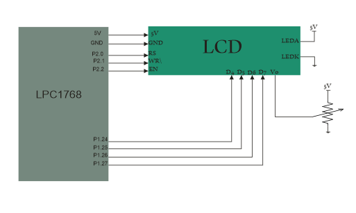
Hardware Connections

Schematic
Below schematic shows the minimum connection required for interfacing the LCD with the microcontroller.
As we are interfacing the LCD in 4-bit mode, only the higher 4 data lines are used as data bus.
Port Connection
This section shows how to configure the GPIO for interfacing the LCD.
The below configuration is as per the above schematic. You can connect the LCD to any of the PORT pins available on your boards and update this section accordingly
LCD Operation
In this section we are going to see how to send the data/cmd to the LCD along with the timing diagrams. First lets see the timing diagram for sending the data and the command signals(RS,RW,EN), accordingly we write the algorithm and finally the code.
Timing Diagram
The below image shows the timing diagram for sending the data to the LCD.
As shown in the timing diagram the data is written after sending the RS and RW signals. It is still ok to send the data before these signals.
The only important thing is the data should be available on the databus before generating the High-to-Low pulse on EN pin.

Steps for Sending Command:
- Send the I/P command to LCD.
- Select the Control Register by making RS low.
- Select Write operation making RW low.
- Send a High-to-Low pulse on Enable PIN with some delay_us.
Steps for Sending Data:
- Send the character to LCD.
- Select the Data Register by making RS high.
- Select Write operation making RW low.
- Send a High-to-Low pulse on Enable PIN with some delay_us.
The timings are similar as above only change is that RS is made high for selecting Data register.
Code Examples
Example 1
Here is the complete code for displaying the data on 2x16 LCD in 4-bit mode.
Using Explore Embedded Libraries :
In the above tutorial we just discussed how to interface 2x16Lcd in 4-bit mode.
Once you know the working of lcd, you can directly use the ExploreEmbedded libraries to play around with your LCD.
For that you need to include the lcd.c/lcd.h and the associated files(delay/stdutils).
After including these files, the only thing you got to do is to configure the PORTs in lcd.h as per your hardware connection.
The below sample code shows how to use the already available LCD functions.
Refer this link for more info on LCD libraries.
Downloads
Download the complete project folder from the below link:
https://codeload.github.com/ExploreEmbedded/Explore-Cortex-M3-LPC1768-Stick-DVB-14001/zip/master
Have a opinion, suggestion , question or feedback about the article let it out here!