Difference between revisions of "A7.8051 Interfacing ADC: LDR & LM35"
| (7 intermediate revisions by the same user not shown) | |||
| Line 45: | Line 45: | ||
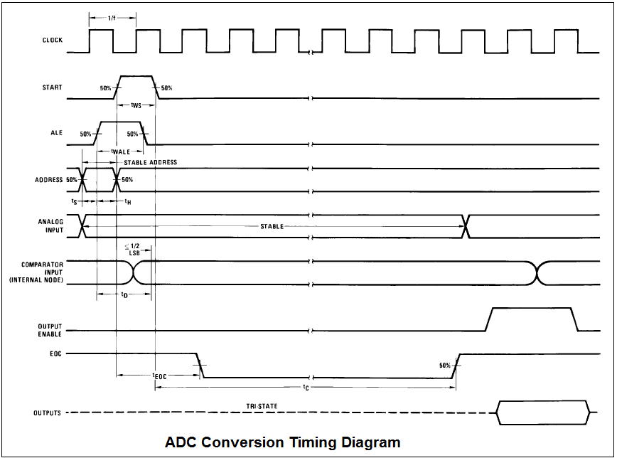
[[File:Adc0809 TimingDiagram.png]] | [[File:Adc0809 TimingDiagram.png]] | ||
| − | = | + | =Pin Connections= |
| − | + | You can connect the ADC0809 to any of the PORT pins available on your boards and update this section accordingly. | |
| − | + | <html><script src="https://gist.github.com/SaheblalBagwan/dd0169a1f593236a66a0575ac3bd5ba2.js"></script></html> | |
| − | + | ||
| − | + | ||
| − | + | ||
| − | + | ||
| − | + | ||
| − | + | ||
| − | + | ||
| − | + | ||
| − | + | ||
| − | + | ||
| − | + | ||
| − | < | + | |
| − | + | =Steps for ADC Conversion= | |
| − | + | #Select the required ADC channel using A,B,C pins. | |
| − | + | #Send a HIGH pulse on ALE for latching the above selected channel. | |
| − | + | #Send a HIGH pulse on Start pin to reset the SAR(Successive Approximation Register). | |
| − | + | #Pull the ALE line low as the address is lateched and futher changes on A,B,C should not change the channel. | |
| − | + | #Pull Start line LOW to start the conversion. | |
| − | + | #Wait for the EOC line go HIGH. | |
| − | + | #Pull the OE line HIGH to bring the conversion data on DataBus. | |
| − | + | #Read the ADC data and pull OE line back to LOW. | |
| − | < | + | #Use the ADC data for further processing |
| − | + | <html><script src="https://gist.github.com/SaheblalBagwan/d47bf4d9abfb1c43a9571e7af9d58000.js"></script></html> | |
| − | + | <br> | |
| − | + | ||
| − | + | ||
| − | + | ||
| − | + | ||
| − | + | ||
| − | + | ||
| − | + | ||
| − | + | ||
| − | + | =Hardware Connection= | |
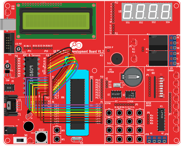
| − | + | [[File:Adc0809 Interafce.png]] | |
| − | + | ||
| − | + | ||
| − | + | ||
| − | + | ||
| − | + | ||
| − | + | ||
| − | + | ||
| − | + | ||
| − | + | ||
| − | + | ||
| − | + | ||
| − | + | ||
| − | + | ||
| − | + | ||
| − | + | ||
| − | + | ||
| − | + | ||
| − | + | ||
| − | + | ||
| − | + | ||
| − | + | ||
| − | + | ||
| − | + | ||
| − | + | ||
| − | + | ||
| − | [[ | + | |
<br><br> | <br><br> | ||
| − | |||
| − | |||
| − | |||
| − | |||
| − | |||
=Code= | =Code= | ||
| − | Below is the sample code to read the ADC value of channel0 and send it | + | Below is the sample code to read the ADC value of channel0 and send it to P0 where the LED's are connected<br> |
<html> | <html> | ||
| − | <script src="https://gist.github.com/SaheblalBagwan/ | + | <script src="https://gist.github.com/SaheblalBagwan/328e438db789f5e73b74603733207fd6.js"></script></script> |
</html> | </html> | ||
=Using ExploreEmbedded Libraries= | =Using ExploreEmbedded Libraries= | ||
| + | Below is the sample code to read the ADC value of channel0 and send it on UART at 9600 baud rate. | ||
<html> | <html> | ||
| − | <script src="https://gist.github.com/ | + | <script src="https://gist.github.com/SaheblalBagwan/45353c7008277f68204abfe09ba7fc7a.js"></script> |
</html> | </html> | ||
| Line 133: | Line 83: | ||
=Downloads= | =Downloads= | ||
Download the complete project folder from the below link:<br> | Download the complete project folder from the below link:<br> | ||
| − | [https://github.com/ExploreEmbedded/ | + | [https://github.com/ExploreEmbedded/8051_DevelopmentBoard Hardware design Files and Code Library] |
Have an opinion, suggestion , question or feedback about the article let it out here! | Have an opinion, suggestion , question or feedback about the article let it out here! | ||
{{DISQUS}} | {{DISQUS}} | ||
Latest revision as of 17:38, 1 September 2016
In this tutorial, we are going to discuss the interfacing of external ADC0808/9 with 8051.
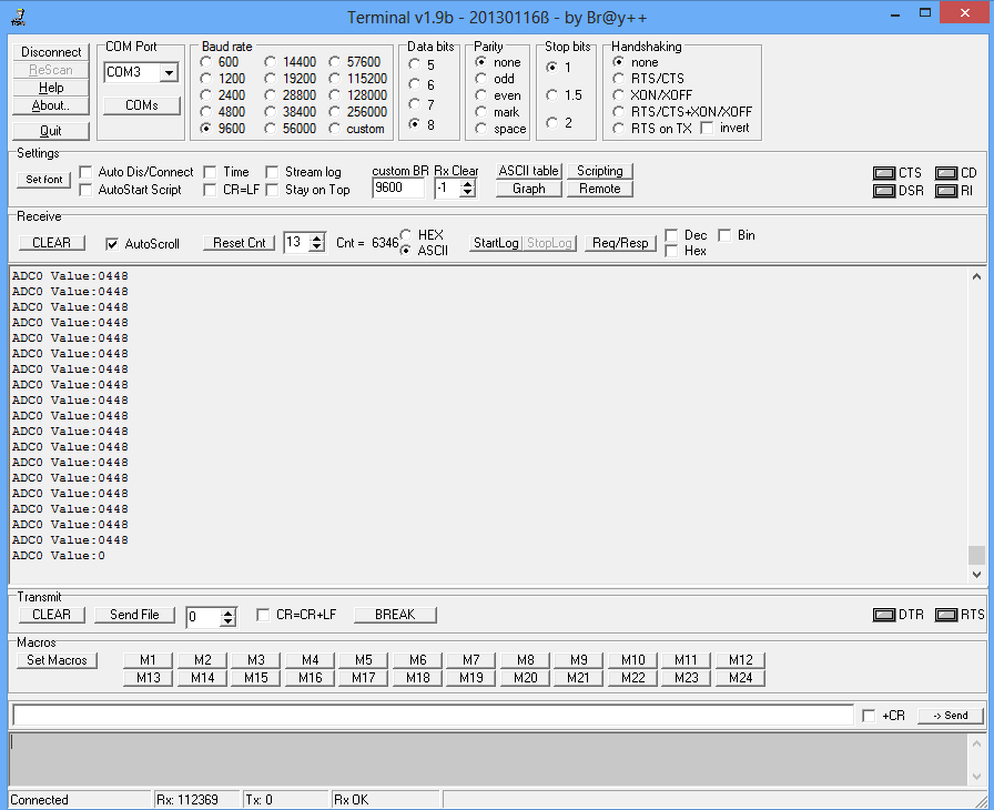
We will be reading the ADC values from channel Zero and transmitted on UART at 9600 baudrate.
Contents
ADC-0808/9
8051 does not have the inbuilt ADC and we will be using the external 8-bit ADC ie. ADC0808/ADC0809.
ADC0809 is an 8-bit Successive Approximation ADC which is multiplexed among 8 input pins.
The A/D module has high and low-voltage reference input that can be set using the pins Vref+ and Vref- as shown in the below image.
With 5v as the Vref+ and 0v as Vref- the resolution of ADC0809 can be determined as below:
$$resolution of ADC = ((Vref+) - (Vref-))/(2^{8}-1) = 5/255 =0.0196 = 19.6mv$$
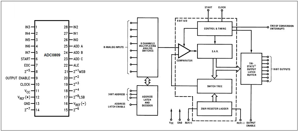
ADC Pins
Lets see the pins of the ADC0809
- Addres Lines(A,B,C): As mentioned earlier, ADC0809 has 8-muliplexed ADC channels. A particular input channel is selected by using these address bits as shown below.
| C | B | A | Selected ADC channel |
|---|---|---|---|
| 0 | 0 | 0 | INO |
| 0 | 0 | 1 | IN1 |
| 0 | 1 | 0 | IN2 |
| 0 | 1 | 1 | IN3 |
| 1 | 0 | 0 | IN4 |
| 1 | 0 | 1 | IN5 |
| 1 | 1 | 0 | IN6 |
| 1 | 1 | 1 | IN7 |
- Address Latch Enable (ALE): A low-to-high signal at this pin will latch the above-selected address and selected the respective channel for ADC conversion.
- START Conversion (SOC): The A/D converter’s successive approximation register (SAR) is reset on the positive edge of the start conversion (SC) pulse. Thus we need to generate a LOW-HIGH-LOW pulse for starting the ADC conversion.
- End of Conversion (EOC): Once the conversion is over, this pin is pulled HIGH by ADC0809. This pin needs to be monitored for the conversion to complete and then read the data.
- Output Enable(OE): ADC0809 does the adc conversion and holds the data in the internal registers. A HIGH signal on this pin will bring the data on the output lines.
Pin Connections
You can connect the ADC0809 to any of the PORT pins available on your boards and update this section accordingly.
Steps for ADC Conversion
- Select the required ADC channel using A,B,C pins.
- Send a HIGH pulse on ALE for latching the above selected channel.
- Send a HIGH pulse on Start pin to reset the SAR(Successive Approximation Register).
- Pull the ALE line low as the address is lateched and futher changes on A,B,C should not change the channel.
- Pull Start line LOW to start the conversion.
- Wait for the EOC line go HIGH.
- Pull the OE line HIGH to bring the conversion data on DataBus.
- Read the ADC data and pull OE line back to LOW.
- Use the ADC data for further processing
Hardware Connection
Code
Below is the sample code to read the ADC value of channel0 and send it to P0 where the LED's are connected
Using ExploreEmbedded Libraries
Below is the sample code to read the ADC value of channel0 and send it on UART at 9600 baud rate.
Downloads
Download the complete project folder from the below link:
Hardware design Files and Code Library
Have an opinion, suggestion , question or feedback about the article let it out here!

