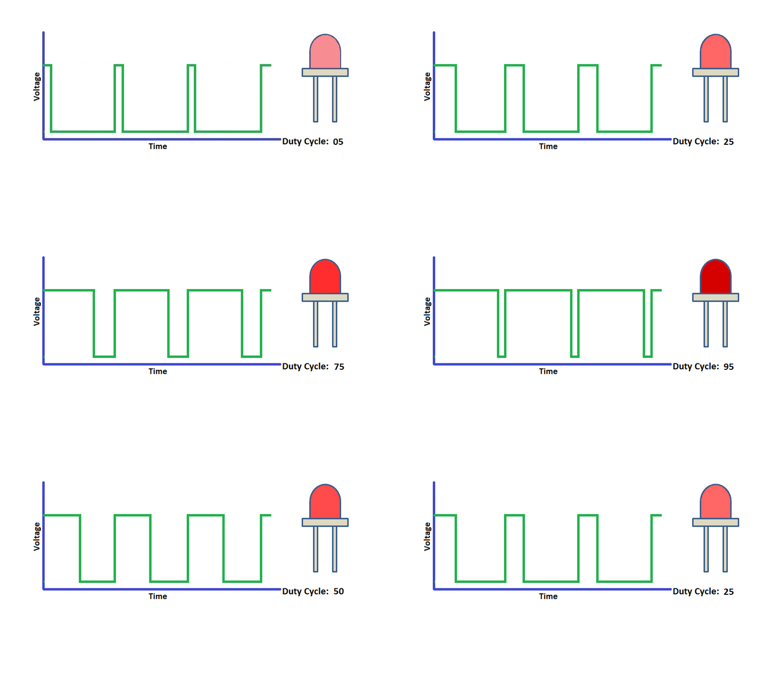
In this tutorial we are going to discuss the PWM module of PIC16F877A.
First we will see how to configure the PWM registers to generate signals of required PWM, At the end we will see how to use the ExploreEmdedded PWM library.
Contents
PIC16F877A PWM Module
PIC16F877A microcontroller has two independent CCP(Capture/Compare/PWM) modules, named as CCP1 and CCP2. Each CCP module has two 8-bit resistors(CCPxH,CCPxL) that can be use as:
- 16 bit Capture Register
- 16 bit Compare Register
- 10-bit PWM Regsietrs .
In this tutorial we will be discussing only the PWM part of CCP. PIC has 2PWM module with a resolution of 10-bits. The 8-Msb bits are stored in CCPRxL and remeining 2-bits in CCPxCON register. Below tables shows the PWM module of PIC.
| PWM Channel | Port Pin | Control Register | Duty Cycle Register |
|---|---|---|---|
| PWM1 | PC.2 | CCP1CON | CCPR1L |
| PWM2 | PC.1 | CCP2CON | CCPR2L |
LPC7168 PWM Registers
The below table shows the registers associated with LPC1768 PWM.
| Register | Description |
|---|---|
| CCPxCON | This register is used to Configure the CCP module for Capture/Compare/PWM opertaion. |
| CCPRxL | This register holds the 8-Msb bits of PWM, lower 2-bits will be part of CCPxCON register. |
| TMR2 | Free running counter which will be compared with CCPR1L and PR2 for generating the PWM output. |
Register Configuration
The below table shows the registers associated with LPC1768 PWM.
| TCR | ||||
|---|---|---|---|---|
| 31:4 | 3 | 2 | 1 | 0 |
| Reserved | PWM Enable | Reserved | Counter Reset | Counter Enable |
Bit 0 – Counter Enable
This bit is used to Enable or Disable the PWM Timer and PWM Prescalar Counters
0- Disable the Counters
1- Enable the Counter incrementing.
Bit 1 – Counter reset
This bit is used to clear the PWM Timer and PWM Prescalar Counter values.
0- Do not Clear.
1- The PWM Timer Counter and the PWM Prescale Counter are synchronously reset on the next positive edge of PCLK.
Bit 3 – PWM Enable
Used to Enable or Disable the PWM Block.
0- PWM Disabled
1- PWM Enabled
| MCR | ||||||||||
|---|---|---|---|---|---|---|---|---|---|---|
| 31:21 | 20 | 19 | 18 | - | 5 | 4 | 3 | 2 | 1 | 0 |
| Reserved | PWMMR6S | PWMMR6R | PWMMR6I | - | PWMMR1S | PWMMR1R | PWMMR1I | PWMMR0S | PWMMR0R | PWMMR0I |
PWMMRxI
This bit is used to Enable or Disable the PWM interrupts when the PWMTC matches PWMMRx (x:0-6)
0- Disable the PWM Match interrupt
1- Enable the PWM Match interrupt.
PWMMRxR
This bit is used to Reset PWMTC whenever it Matches PWMRx(x:0-6)
0- Do not Clear.
1- Reset the PWMTC counter value whenever it matches PWMRx.
PWMMRxS
This bit is used to Stop the PWMTC,PWMPC whenever the PWMTC matches PWMMRx(x:0-6).
0- Disable the PWM stop o match feature
1- Enable the PWM Stop feature. This will stop the PWM whenever the PWMTC reaches the Match register value.
| PCR | ||||
|---|---|---|---|---|
| 31:15 | 14-9 | 8-7 | 6-2 | 1-0 |
| Unused | PWMENA6-PWMENA1 | Unused | PWMSEL6-PWMSEL2 | Unused |
PWMSELx
This bit is used to select the single edged and double edge mode form PWMx (x:2-6)
0- Single Edge mode for PWMx
1- Double Edge Mode for PWMx.
PWMENAx
This bit is used to enable/disable the PWM output for PWMx(x:1-6)
0- PWMx Disable.
1- PWMx Enabled.
| LER | |||||||
|---|---|---|---|---|---|---|---|
| 31-7 | 6 | 5 | 4 | 3 | 2 | 1 | 0 |
| Unused | LEN6 | LEN5 | LEN4 | LEN3 | LEN2 | LEN1 | LEN0 |
LENx
This bit is used Enable/Disable the loading of new Match value whenever the PWMTC is reset(x:0-6)
PWMTC will be continously incrementing whenever it reaches the PWMMRO, timer will be reset depeding on PWMTCR configuraion.
Once the Timer is reset the New Match values will be loaded from MR0-MR6 depending on bits set in this register.
0- Disable the loading of new Match Values
1- Load the new Match values from MRx when the timer is reset.
PWM Working
After looking into the PWM registers, its time to see how the LPC1768 PWM module works.
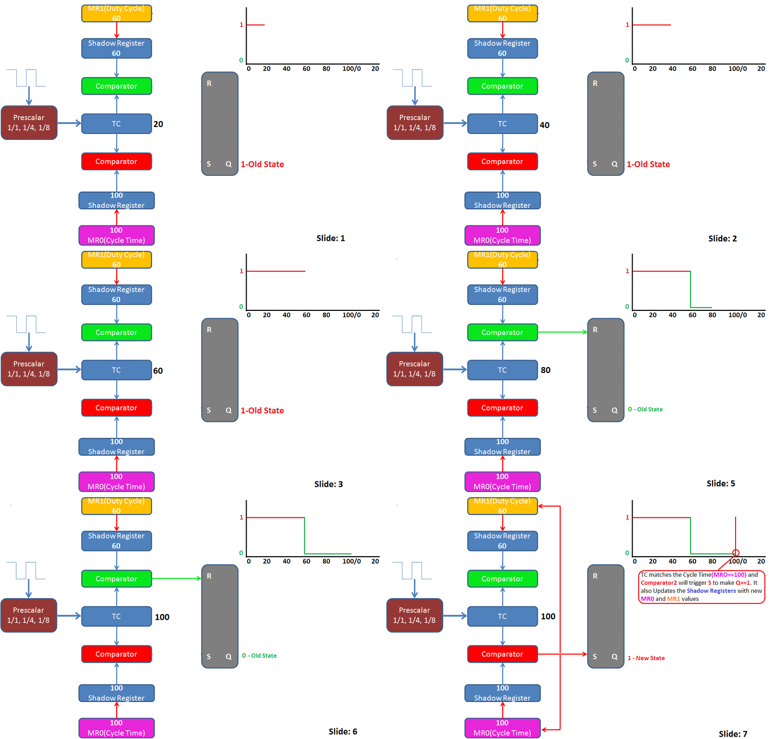
The TC is continuously incremented and once it matches the MR1(Duty Cycle) the PWM pin is pulled Low. TC still continues to increment and once it reaches the Cycle time(Ton+Toff) the PWM module does the following things:
- Reset the TC value.
- Pull the PWM pin High.
- Loads the new Match register values.
Summary of PWM operations for the above image:
- Slide1: The TC is being incremented as per the Pre-scalar configuration. The PWM output is high as the TC is still less that duty cycle.
- Slide2: TC is incremented to 40 and still the PWM pin as HIGH.
- Slide3: TC is incremented to 60 and it matches the Duty Cycle(MR1=60).
- Slide4: Now the Comparator1(Green) will trigger the R of SR latch and Pulls the PWM output to Zero(Q=0). TC still continues to increment.
- Slide5: TC is incremented to 80 and PWM pin is low as TC>Duty Cycle.
- Slide6: Now TC is 100 and it matches the Cycle time(MR0==100).
- Slide7: Now the Comparator2(Red) will trigger the S of SR latch and pulls the PWM output to ONE(Q==1). It also resets the TC to zero. It updates Shadow buffers with new Match values from MRO,MR1.
Steps to Configure PWM
- Configure the GPIO pins for PWM operation in respective PINSEL register.
- Configure TCR to enable the Counter for incrementing the TC, and Enable the PWM block.
- Set the required pre-scalar value in PR. In our case it will be zero.
- Configure MCR to reset the TC whenever it matches MR0.
- Update the Cycle time in MR0. In our case it will be 100.
- Load the Duty cycles for required PWMx channels in respective match registers MRx(x: 1-6).
- Enable the bits in LER register to load and latch the new match values.
- Enable the required pwm channels in PCR register.
Example
Program to demonstrates the variable PWM signal generation on PWM_1-PWM_4(P2_0 - P2_3).
Connect the Leds to the pins P2_0 to P2_3 and observe the led brigthness change depending on the dutycycle.


