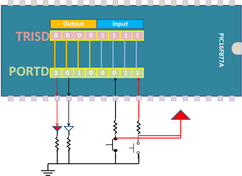
In this tutorial we are going to discuss the port configuration of PIC controllers. In this tutorial we will be using PIC16F877A as reference, same will be applicable for other PIC series controllers.
At the end of this tutorial you will be familiar with the PIC GPIO's and the associated registers for configuring and accessing the GPIO's.
GPIO Registers
The basic and important feature of any controllers is the number of gpio's available for connecting the peripherals. PIC16F877A has 33-gpio's grouped into five ports namely PORTA-PORTE as shown in the below table.
| PORT | Direction Register | Number of Pins | Alternative Function |
| PORTA | TRISA | 6 (PA0-PA5) | ADC |
| PORTB | TRISB | 8 (PB0-PB7) | Interrupts |
| PORTC | TRISC | 8 (PC0-PC7) | UART,I2C,PWM |
| PORTD | TRISD | 8 (PD0-PD7) | Parallel Slave Port |
| PORTE | TRISE | 3 (PE0-PB2) | ADC |
As shown in the above table many I/O pins have 2-3 functions. If a pin is used for other function then it may not be used as a gpio.
Though the gpio pins are grouped into 8-bit ports they can still be configured and accessed individually.
Each Port is associated with 2 registers for direction configuration(Input/Output) and for Read/Write.

| Register | Description |
| TRISx | Used to configure the respective PORT as output/input |
| PORTx | Used to Read/Write the data from/to the Port pins |
note: Here 'x' could be A,B,C,D,E so on depending on the number of ports supported by the controller.
TRISx:TRI-State Register/ Data Direction Register
Before reading or writing the data from the ports, their direction needs to be set. Unless the PORT is configured as output, the data from the registers will not go to controller pins.
This register is used to configure the PORT pins as Input or Output. Writing 1's to TRISx will make the corresponding PORTx pins as Input. Similarly writing 0's to TRISx will make the corresponding PORTx pins as Output.
TRISB = 0xff;  // Configure PORTB as Input.

TRISC = 0x00; // Configure PORTC as Output.

TRISD = 0x0F; // Configure lower nibble of PORTD as Input and higher nibble as Output

TRISD = (1<<0) | (1<3) | (1<<6); // Configure PD0,PD3,PD6 as Input and others as Output
PORTx:
This register is used to read/write the data from/to port pins. Writing 1's to PORTx will make the corresponding PORTx pins as HIGH. Similarly writing 0's to PORTx will make the corresponding PORTx pins as LOW.
Before reading/writing the data, the port pins should be configured as InputOutput.
PORTB = 0xff;  // Make all PORTB pins HIGH.

PORTC = 0x00;  // Make all PORTC pins LOW..

PORTD = 0x0F;  // Make lower nibble of PORTD as HIGH and higher nibble as LOW

PORTD = (1<<PD0) | (1<PD3) | (1<<PD6); // Make PD0,PD3,PD6 HIGH,


TRISB = 0x00;  // Configure PORTB as Output
TRISD = 0xff;  // Configure PORTD as Input
PORTD = PORTB; // Read the data from PORTB and send it to PORTD.
Led Blinking Example
After knowing how to configure the GPIO ports, its time to write a simple program to blink the Leds.
- Configure the PORTS as outputs using TRIS registers.
- Turn ON all the LEDs and wait for some time.
- Turn OFF all the LEDs and wait for some time.
Led and Switches
Downloads
Download the complete project folder from the below link:
Hardware design Files and Code Library
Have a opinion, suggestion , question or feedback about the article let it out here!
