Difference between revisions of "5.8051 Timer programming"
| Line 66: | Line 66: | ||
|} | |} | ||
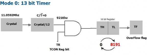
[[File:Mode_0.jpeg|thumbnail|600xpx|fig 2:Mode 0]] | [[File:Mode_0.jpeg|thumbnail|600xpx|fig 2:Mode 0]] | ||
| − | [[File:Mode_1.jpeg|thumbnail|600xpx|fig 3:Mode 1]] | + | [[File:{{#setmainimage: Mode_1.jpeg}}|thumbnail|600xpx|fig 3:Mode 1]] |
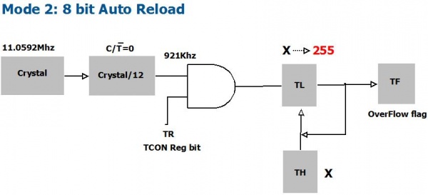
[[File:Mode_2.jpeg|thumbnail|600xpx|fig 4:Mode 2]] | [[File:Mode_2.jpeg|thumbnail|600xpx|fig 4:Mode 2]] | ||
Revision as of 07:32, 27 December 2013
In this tutorial we will see 8051 timers. We will use the 8051 timers to generate a precise delay of 1 sec.
Contents
8051 timers/counters
The 8051 has 2 timers/counters.
- They can be used to generate precise timing, i.e., we can measure time between events. The unit is then called timer.
- It can also be used to count external events, known as counter.
- Timer 1 is also used for generating baud rate in serial communication, which we will discuss in the next tutorial
Timer Operation
The Timer 0 is a 16 bit registers as shown. This can be accessed as 2 eight bit registers TL0 and TL1. Same applies to Timer 1.
The 8051 timer and counter is the same unit, but in this tutorial we will discuss only the timer unit to simplify the discussion.
The 8051 timer and counter is the same unit, but in this tutorial we will discuss only the timer unit to simplify the discussion.
Timer Tick
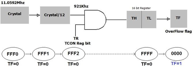
Fig 1, shows the basic 8051 timer unit. The registers TCON and TMOD affect the timer operation. The clock frequency is divided by 12 and used by the timer unit. Thus if a 11.0592MHz external crystal is used, the timer uses a frequency of 921KHz. Thus timer increments every 1.085μ seconds.
- The C/Ṫ = 0 bit of TMOD register selects operation of Timer/counter unit as timer.
- The TR bit of TCON register is used to start the timer.
Timer Registers
Timer Register T0/T1
| T0 | |||||||||||||||
|---|---|---|---|---|---|---|---|---|---|---|---|---|---|---|---|
| TH0 | TL0 | ||||||||||||||
| D15 | D14 | D13 | D12 | D11 | D10 | D9 | D8 | D7 | D6 | D5 | D4 | D3 | D2 | D1 | D0 |
TMOD Register
The TMOD Register specifies the operational mode of the two timers. The higher nibble is used for Timer 1 and Lower for the timer 0 as shown below.
| M1 | M0 | Operation |
|---|---|---|
| 0 | 0 | 13 bit Timer |
| 0 | 1 | 16 bit Timer |
| 1 | 0 | 8 bit Auto Reload |
| 1 | 1 | Split Mode |
| TMOD | |||||||
|---|---|---|---|---|---|---|---|
| D7 | D6 | D5 | D4 | D3 | D2 | D1 | D0 |
| Gate | C/T | M1 | M0 | Gate | C/T | M1 | M0 |
| Timer1 | Timer 0 | ||||||
TCON Register
| TCON | |||||||
|---|---|---|---|---|---|---|---|
| D7 | D6 | D5 | D4 | D3 | D2 | D1 | D0 |
| TF1 | TR1 | TF0 | TR0 | IE1 | IT1 | IE0 | IT0 |
| Timer1 | Timer 0 | Timer Interrupts | |||||


