Difference between revisions of "AVR I/O Register Configuration"
| Line 104: | Line 104: | ||
</html> | </html> | ||
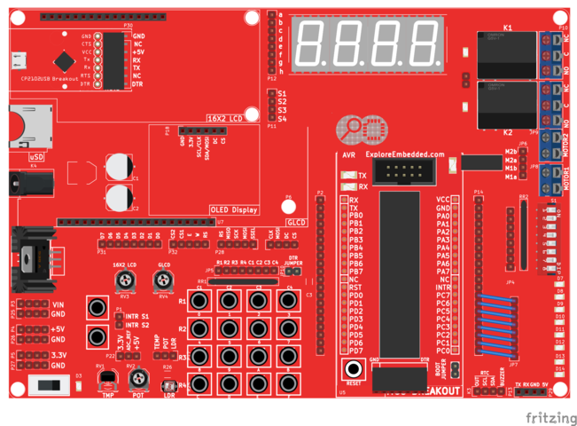
==Wiring diagram== | ==Wiring diagram== | ||
| − | [[File:Blink | + | [[File:Blink bb.png|x480px|center]] |
=Led and Switches= | =Led and Switches= | ||
Revision as of 15:02, 4 February 2016
Objective
In this tutorial we are going to discuss the port configuration of AVR/Atmel controllers or in general Atmega family. In this tutorial we will be using Atmega32 as reference, same will be applicable to other Atmega series controllers.
At the end of this tutorial you will be familiar with the Atmega GPIO's and the associated registers for configuring and accessing the GPIO's.
GPIO Registers
The basic and important feature of any controllers is the number of gpio's available for connecting the peripherals. Atmega32 has 32-gpio's grouped into four 8-bit ports namely PORTA-PORTD as shown in the below image.
As shown in the above image many I/O pins have 2-3 functions. If a pin is used for other function then it may not be used as a gpio.
Though the gpio pins are grouped into 8-bit ports they can still be configured and accessed individually.
Each Port is associated with 3 registers for direction configuration(Input/Output), read and write operation.
| Register | Description |
|---|---|
| DDRx | Used to configure the respective PORT as output/input |
| PORTx | Used to write the data to the Port pins |
| PINx | Used to Read the data from the port pins |
DDRx: Data Direction Register
Before reading or writing the data from the ports, their direction needs to be set. Unless the PORT is configured as output, the data from the registers will not go to controller pins.
This register is used to configure the PORT pins as Input or Output. Writing 1's to DDRx will make the corresponding PORTx pins as output. Similarly writing 0's to DDRx will make the corresponding PORTx pins as Input.
DDRB = 0xff;  // Configure PORTB as Output.

DDRC = 0x00; // Configure PORTC as Input.

DDRD = 0x0F; // Configure lower nibble of PORTD as Output and higher nibble as Input

DDRD = (1<<PD0) | (1<PD3) | (1<<PD6); // Configure PD0,PD3,PD6 as Output and others as Input
PORTx:
This register is used to send the data to port pins. Writing 1's to PORTx will make the corresponding PORTx pins as HIGH. Similarly writing 0's to PORTx will make the corresponding PORTx pins as LOW.
PORTB = 0xff;  // Make all PORTB pins HIGH.

PORTC = 0x00; // Make all PORTC pins LOW..

PORTD = 0x0F; // Make lower nibble of PORTD as HIGH and higher nibble as LOW

PORTD = (1<<PD0) | (1<PD3) | (1<<PD6); // Make PD0,PD3,PD6 HIGH,
PINx:PORT Input Register
This register is used to read the data from the port pins. Before reading the data from the port pins, the ports needs to be configured as Inputs.
DDRB  = 0x00; // Configure the PORTB as Input.
value = PINB;  // Read the data from PORTB.


DDRB = 0x00; // Configure PORTB as Input
DDRD = 0xff;  // Configure PORTD as Output
PORTD = PINB; // Read the data from PORTB and send it to PORTD.
Enabling Internal Pull Up Resistors:
Making the DDRx bits to 0 will configure the PORTx as Input. Now the corresponding bits in PORTx register can be used to enable/disable pull-up resistors associated with that pin.To enable pull-up resistor, set bit in PORTx to 1, and to disable set it to 0.
DDRB  = 0x00;  // Configure the PORTB as Input.
PORTB = 0xFF;  // Enable the internal Pull Up resistor of PORTB.

DDRD = 0xff;  // Configure PORTD as Output
PORTD = PINB; // Read the data from PORTB and send it to PORTD.
Led Blinking Example
After knowing how to configure the GPIO ports, its time to write a simple program to blink the Leds.
Below points needs to be considered for this example.
- Include the io.h file as it has the definitions for all the PORT registers.
- Include delay.h file to use the delay functions.
- Configure the PORT as Output before writing any data to PORT pins.
Wiring diagram
Led and Switches

