Difference between revisions of "1.8051 Architecture"
(→READ 1) |
|||
| Line 1: | Line 1: | ||
| + | [[Category:8051_tutorials]] | ||
{{Box|type=green_light|text=8051 Architecture}} | {{Box|type=green_light|text=8051 Architecture}} | ||
=====Introduction===== | =====Introduction===== | ||
Revision as of 10:56, 26 March 2014
Contents
Introduction

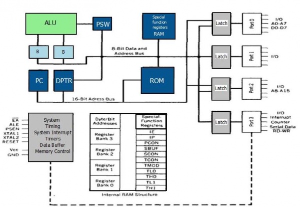
As we have seen in the Previous tutorial, it basically consists of a ALU, RAM, ROM, IO Ports, Timers/Counters, Serial Port and Interrupt Structure. Well, it also has some internal resisters.
Let us start discussing the ALU, as it is the main unit. Understanding of ALU, will allow us to put other units in their place.
Arithmetic and Logical Unit (ALU)
ALU performs arithmetic like addition, subtraction, multiplication and Logical Operations like NAND, NOR etc. Since 8051 is an 8 bit microcontroller, it takes input from two 8 bit registers namely A and B and processes them. If would like a deeper insight as to how an ALU is built from basic building blocks(logic gates) you may go refer to this tutorial:(4 bit ALU in detail). It would give you a deeper understanding of the microcontrollers, and it it would link your basic concepts like logical gates to the microcontrollers.
Registers of 8051
8 bit Registers
The commonly used registers are R0 to R7, A, B, PSW These are all 8 bit registers. The registers associated with the ALU are A,Band PSW. In most operations, ALU performs specified operation on registers 'A' and 'B' and the result is stored back in 'A'. Hence Register 'A' is often called accumulator.
Program Status Word
'PSW' indicates various flags associated with the operation performed. Figure below shows the 8 bits of the PSW register and their function is shown in the table.
| CY | Carry Flag |
| AC | |
| F0 | Available for general use |
| RS1 | Register Bank Selection bit 1 |
| RS0 | Register Bank Selection bit 0 |
| OV | Overflow flag |
| * | User Definable bit |
| P | Parity flag |
16 bit Registers.
There are also some 16 bit registers in 8051 as shown in the figure. The program counter points to the next instruction that the CPU executes.
The DPTR and other special function registers like SCON, TCON,P0,P1,P2 etc will be discussed while using microcontroller features like timers, counter, serial communication, Interrupts etc.
Internal RAM in Detail
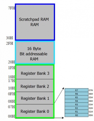
Figure Below show Internal RAM of 8051 it is divided into 3 main sections:
1. Register Banks
- There are 32 8-bit registers arranged in 4 groups. These are used as general purpose registers.
2. Bit Addressable RAM
- 8051 has 16 bytes of RAM, which is bit addressable. It is grouped as 16, 8 byte arrays and any of the 128 bits can also be set/cleared individually.
3. Scratch PAD RAM
- The third group of registers occupy addresses 2Fh-7Fh, i.e. 80 locations, and does not have any special functions or features. Scratch pad RAM is used by the ALU, while fetching, decoding and executing the instructions during operation of the microcontroller.
System Timing, Interrupts, Timers, Data Buffers and Memory Control
- System Timing, refers to the entire timing unit of the microcontroller. The primary source of timing for 8051 is external crystal. The system timing unit is mainly responsible for providing timing to critical events like instruction fetch, decode and execute operations.
- Interrupts: 8051 provides a method to stop current execution and switch over to a priority task with the use of Interrupts. They are associated with external pins P3.2(INT0) and P3.3(INT1). As well as internal units like timers and serial communication. Thus an interrupt to 8051 can be external generated by peripheral device or internal from one of its inbuilt units sometimes referred as software interrupt.
- Timers/Counters: Again one of the most widely used features, timers are used to count time internally or can be made to count external event as counters.
- Memory Control: It is an internal unit of the microcontroller, responsible for accessing data from RAM and ROM.
We will discuss Interrupts, Timers, counters, and Serial Communication in detail with concrete examples in upcoming tutorials.
PIN Diagram and IO port structure
Figure 1 shows the pin diagram of a 8052(only difference is that it has some addition features). In fact we will be using either a AT89S52 OR P89V51RD2 in our interfacing tutorials. As we can see there are four 8 bit ports P0,P1,P2 and P3.
All the ports can be used either as input and output. You would also observe some of the pins have additional functions. We will discuss additional features with relevant topics.
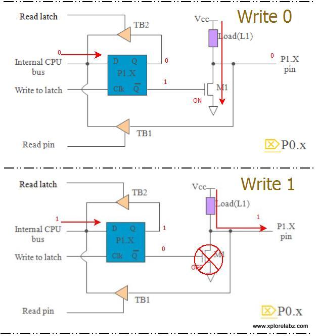
Input/Output pins are widely used to interface a microcontroller with the external peripherals, like LEDs, SevenSegments, LCDs, Motors and the list goes on. Although most of the peripherals are not connected directly, it is essential to understand the way in which micro-controller, reads or writes bits to the port pins. The micrcontroller sends and receives binary 1s or 0s on each of the pins. All the four ports are similar, expect P0 which deos not have internal pull up.

WRITE 0
 To write 0 to pin of the microcontroller:
- Write a '0' to pin: The D latch output is one, the mosfet M1 is turned ON output is grounded as shown in the figure
WRITE 1
To write 1 to pin of the microcontroller:
- Write a '1' to pin: The D latch output is zero, the mosfet M1 is turned OFF output is 1 as shown in the figure
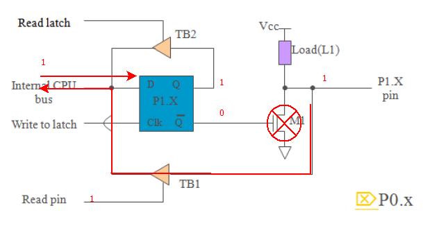
READ 0
 To read 0 from the pin of the microcontroller:
- Write one to pin.
- M1 turns OFF
- Read PIN latch is turned ON
- External zero grounds the pin.
READ 1
{{#seo: |title=8051_Architecture |titlemode=append |keywords=8051,AT89s51,at89c51,p89v51rd2,RAM,ALU,Register,Program status word,Timing,Timer,Interrupts,Data buffers,Memory Control,IO port,xplorelabz,tutorials,8051 basics,ports |description= 8051 Architecture }}
Would like to have your feedback and suggestions here;


