Difference between revisions of "ADC Using PIC16F877A"
| Line 36: | Line 36: | ||
|4|| RE2 || AN7 | |4|| RE2 || AN7 | ||
|}<br><br> | |}<br><br> | ||
| + | |||
| + | =ADC Registers= | ||
| + | |||
| + | |||
| + | =x= | ||
| + | |||
| + | =y= | ||
=Code= | =Code= | ||
Revision as of 14:19, 5 May 2016
In this tutorial we are going to discuss how to use the inbuilt PIC16f877A ADC.
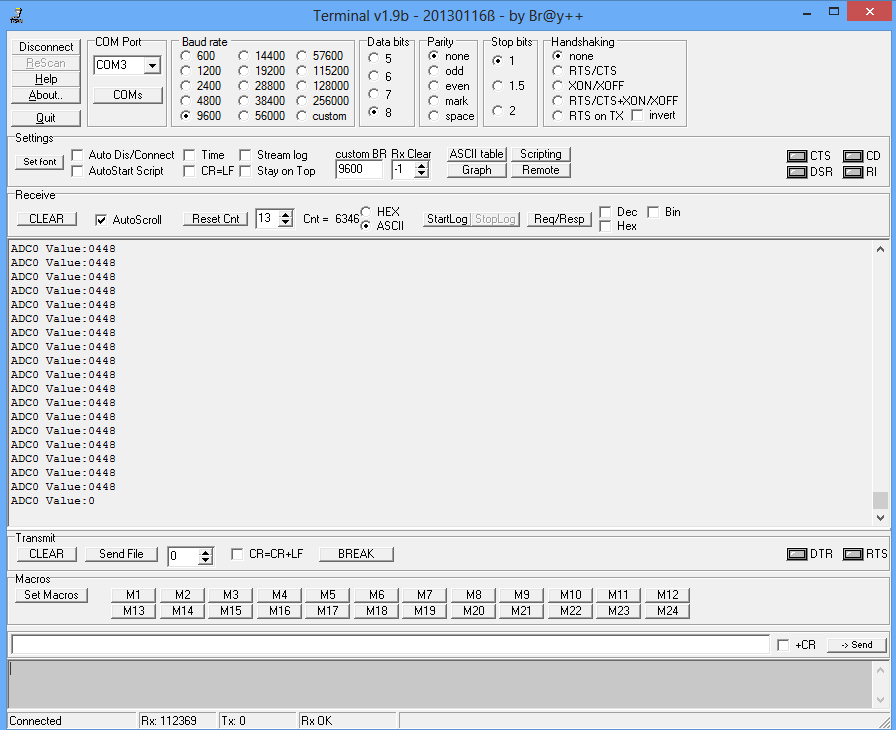
We will be reading the ADC values from chanel Zero and transmitted on UART at 9600 baudrate.

Contents
PIC16F877A ADC pins
PIC16F877A has an inbuilt 10 bit Successive Approximation ADC which is multiplexed among 8 input pins.
The A/D module has high and low-voltage reference input that is software selectable to some combination of VDD, VSS, RA2 or RA3.
With 5v as the Vref the resolution of Pic16f877a ADC can be determined as below:
$$resolution of ADC = Vref/(2^{10}) = 5/1024 =0.00488 = 4.9mv$$
The below table shows the ADC input pins multiplexed with other GPIO pins.
The ADC pin can be enabled by configuring the corresponding ACON1 register.
When the ADC function is selected for a pin ,then other Digital signals are disconnected from the ADC input pins.
| Adc Channel | Pic16f877a Pin | Pin Function |
|---|---|---|
| 0 | RA0 | AN0 |
| 1 | RA1 | AN1 |
| 2 | RA2 | AN2/VREF- |
| 3 | RA3 | AN3/VREF+ |
| 4 | RA5 | AN4 |
| 2 | RE0 | AN5 |
| 3 | RE1 | AN6 |
| 4 | RE2 | AN7 |
ADC Registers
x
y
Code
Below is the sample code to read the ADC value of channel0 and sent it on UART at 9600 baud rate.
As the POT is connected to ADC0, the values can be varied using this POT.

