Difference between revisions of "1.8051 Architecture"
| Line 16: | Line 16: | ||
{{Box|type=l_green_light|text=<br /> | {{Box|type=l_green_light|text=<br /> | ||
The registers associated with the CPU are '''A''','''B'''and '''PSW'''. In most operations, ALU performs specified operation on registers 'A' and 'B' and the result is stored back in 'A'. Hence Register 'A' is often called accumulator.'PSW' indicates various flags associated with the operation performed. | The registers associated with the CPU are '''A''','''B'''and '''PSW'''. In most operations, ALU performs specified operation on registers 'A' and 'B' and the result is stored back in 'A'. Hence Register 'A' is often called accumulator.'PSW' indicates various flags associated with the operation performed. | ||
| + | There are various other registers like PC, DPTR, etc associated with CPU and several others like SCON, PORTA, etc with internal and external units of the microcontroller. We will discuss them while interfacing in the subsequent tutorials. | ||
}} | }} | ||
Revision as of 11:10, 11 December 2013
8051 Architecture
Contents
Introduction
In this tutorial we will discuss, the internal architecture of 8051. Well, not to worry; we will break it down in smaller pieces to understand it. I think a basic understand of Digital electronics would help. Nonetheless, for using 8051 in interfaces and applications, you might just go through it once. Being said that, a through understand will not only help in understand microcontrollers in depth, but will also help in programming efficiently.


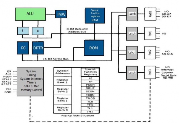
As we have seen in the Previous tutorial, it basically consists of a ALU, RAM, ROM, IO Ports, Timers/Counters, Serial Port and Interrupt Structure. Well, it also has some internal resisters.
Let us start discussing the ALU, as it is the main unit. Understanding of ALU, will allow us to put other units in their place.
Arithmetic and Logical Unit (ALU)
ALU performs arithmetic like addition, subtraction, multiplication and Logical Operations like NAND, NOR etc. Since 8051 is an 8 bit microcontroller, it takes input from two 8 bit registers namely A and B and processes them. If would like a deeper insight as to how an ALU is built from basic building blocks(logic gates) you may go refer to this tutorial:(4 bit ALU in detail). It would give you a deeper understanding of the microcontrollers, and it it would link your basic concepts like logical gates to the microcontrollers.
Registers of 8051
The registers associated with the CPU are A,Band PSW. In most operations, ALU performs specified operation on registers 'A' and 'B' and the result is stored back in 'A'. Hence Register 'A' is often called accumulator.'PSW' indicates various flags associated with the operation performed. There are various other registers like PC, DPTR, etc associated with CPU and several others like SCON, PORTA, etc with internal and external units of the microcontroller. We will discuss them while interfacing in the subsequent tutorials.
Internal RAM in Detail
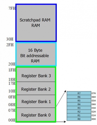
Figure Below show Internal RAM of 8051 it is divided into 3 main sections:
1. Register Banks
- There are 32 8-bit registers arranged in 4 groups. These are used as general purpose registers.
2. Bit Addressable RAM
- 8051 has 16 bytes of RAM, which is bit addressable. It is grouped as 16, 8 byte arrays and any of the 128 bits can also be set/cleared individually.
3. Scratch PAD RAM
- The third group of registers occupy addresses 2Fh-7Fh, i.e. 80 locations, and does not have any special functions or features.
System Timing, Interrupts, Timers, Data Buffers and Memory Cotrol
IO port structure

