Difference between revisions of "LPC1768: Keil Project For Bin File"
(4 intermediate revisions by the same user not shown) | |||
Line 27: | Line 27: | ||
<html> | <html> | ||
<script src="https://gist.github.com/SaheblalBagwan/cb2cf78aadc724737d79.js"></script> | <script src="https://gist.github.com/SaheblalBagwan/cb2cf78aadc724737d79.js"></script> | ||
+ | </html> | ||
+ | <br> | ||
+ | <html> | ||
+ | <script src="https://gist.github.com/SaheblalBagwan/fe401523c97e4cb2d7e98565e1bd3b06.js"></script> | ||
</html> | </html> | ||
<br> | <br> | ||
Line 49: | Line 53: | ||
[[File:Lpc1768_Keil_13.png]]<br><br> | [[File:Lpc1768_Keil_13.png]]<br><br> | ||
− | <b>Step14:</b> Set IROM1 start address as 0x2000. Bootloader will be stored from 0x0000-0x2000 so application | + | <b>Step14:</b> Set IROM1 start address as 0x2000. Bootloader will be stored from 0x0000-0x2000 so application should start from 0x2000<br> |
[[File:Lpc1768_Keil_21.png]]<br><br> | [[File:Lpc1768_Keil_21.png]]<br><br> | ||
Line 66: | Line 70: | ||
<br><br> | <br><br> | ||
− | =Uploading the | + | =Uploading the Bin file= |
− | After generating the .bin file check | + | After generating the .bin file check this tutorial for [[LPC1768: Uploading Hex and Bin files|Uploading Hex and Bin files.]]. |
<br><br> | <br><br> | ||
Latest revision as of 16:35, 27 October 2017
Contents
[hide]Objective
In this tutorial we will see how to setup a keil project to generate .bin file for LPC1768
Keil Setup Steps
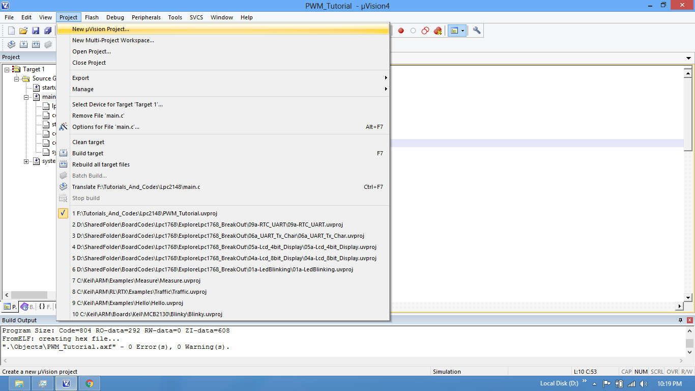
Step1: Open the Keil software and select the New Microvision project from Project Menu as shown below.
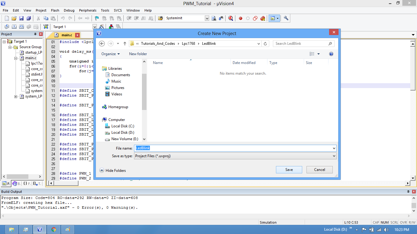
Step2: Browse to your project folder and provide the project name and click on save.
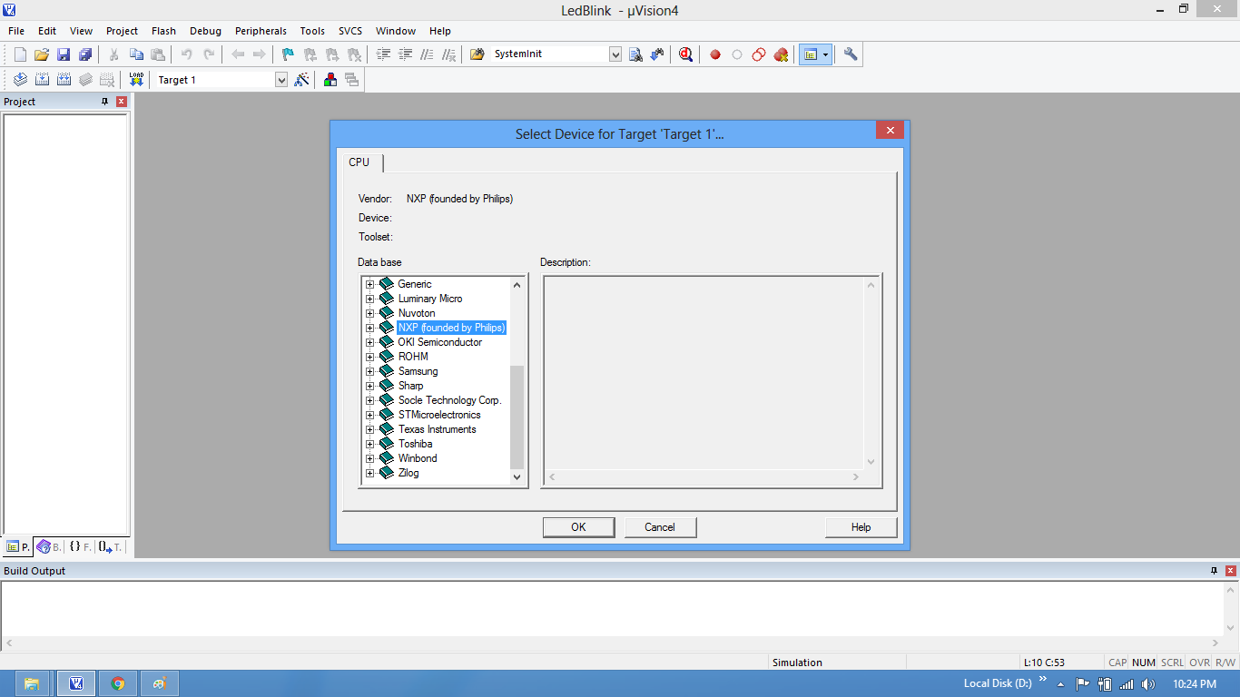
Step3: Once the project is saved a new pop up “Select Device for Target” opens, Select the controller(NXP:LPC1768) and click on OK.
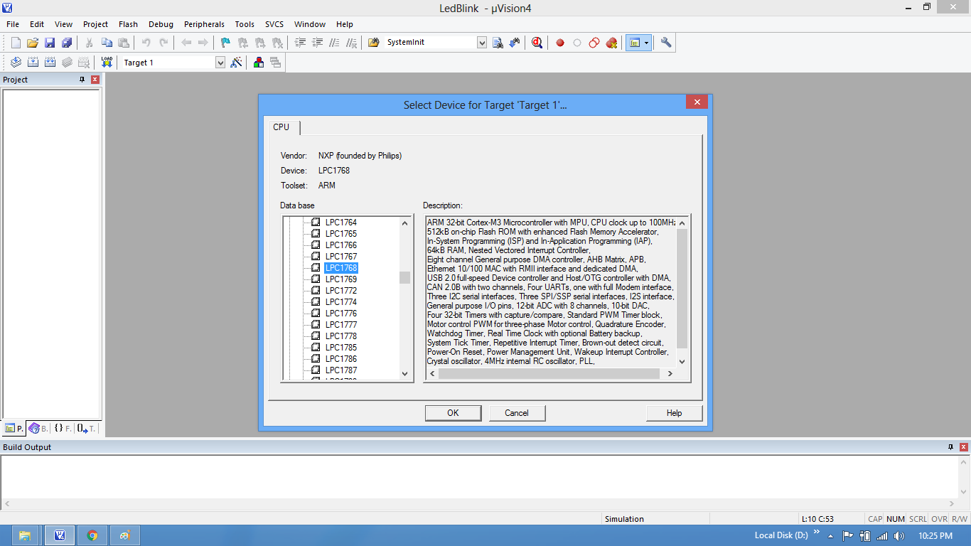
Step4: Select the controller(NXP:LPC1768) and click on OK.
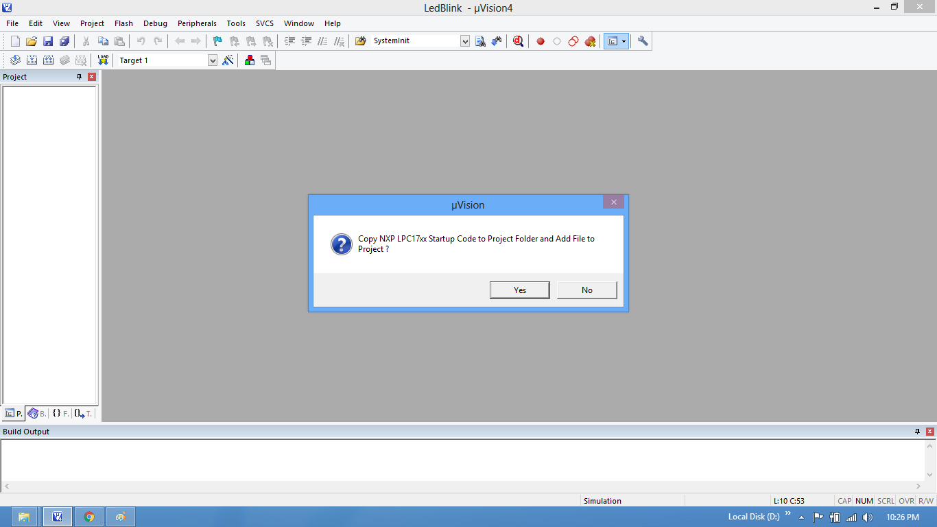
Step5: As LPC1768 needs the startup code, click on Yes option to include the LPC17xx Startup file.
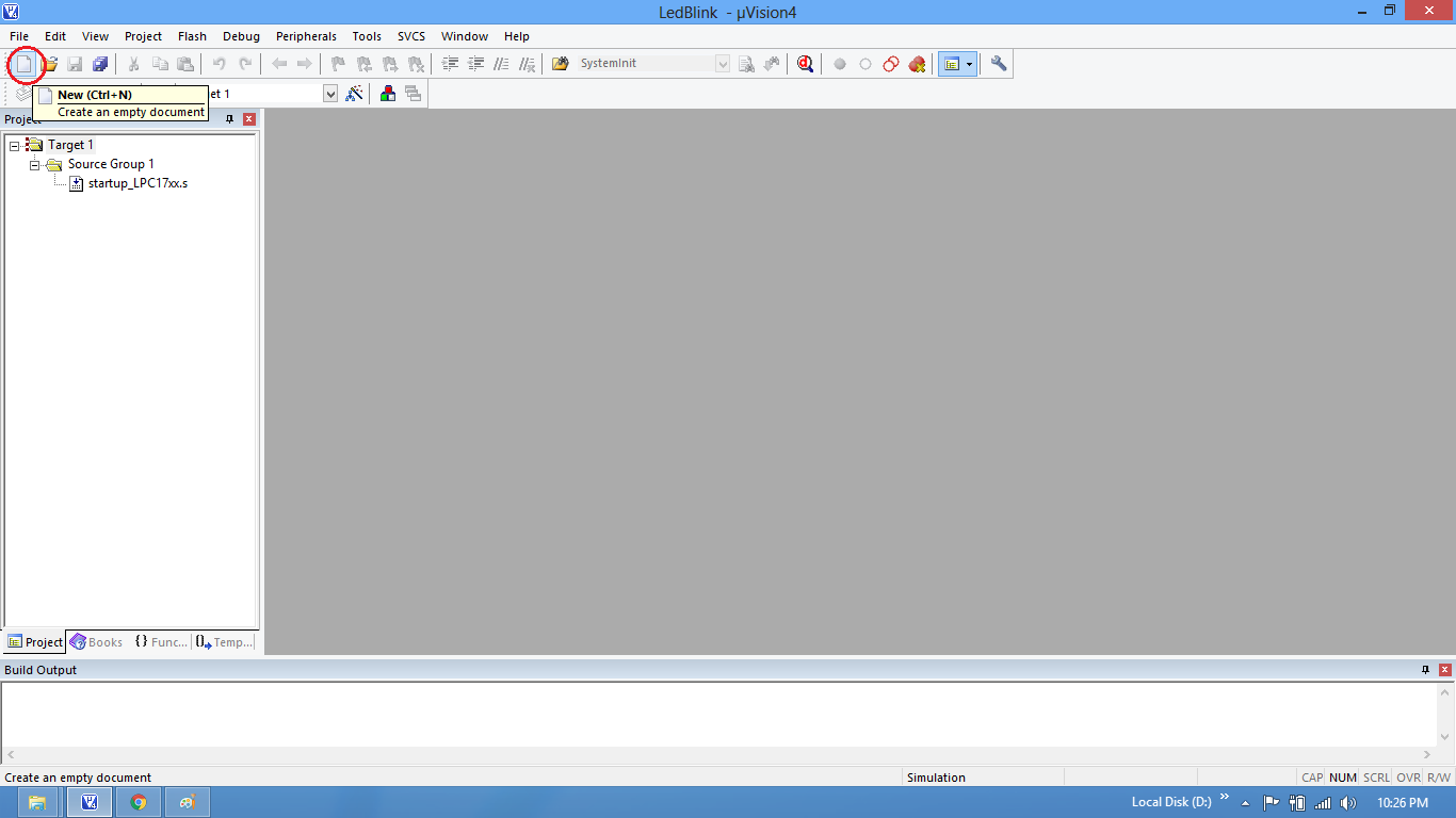
Step6: Create a new file to write the program.
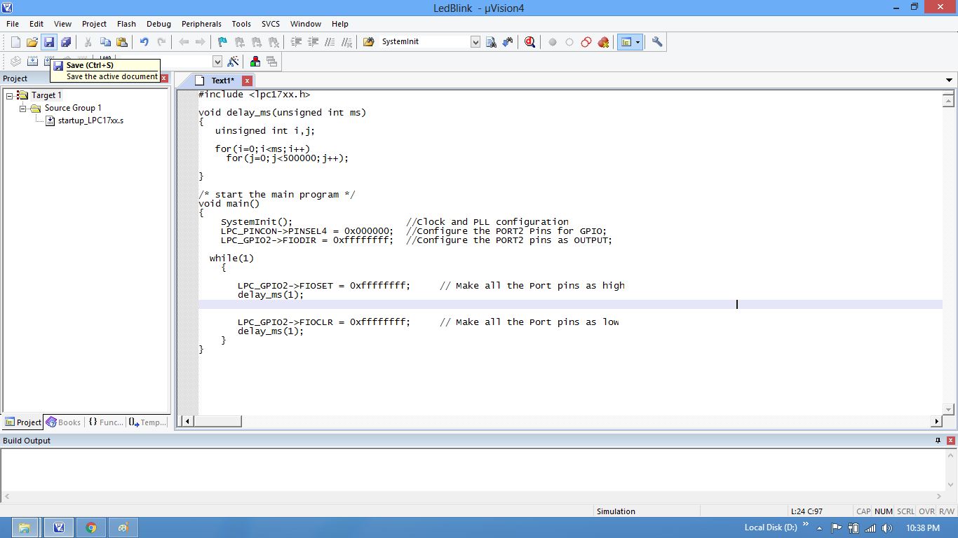
Step7: Type the code or Copy paste the below code snippet.
#include <lpc17xx.h> | |
void delay_ms(unsigned int ms) | |
{ | |
unsigned int i,j; | |
for(i=0;i<ms;i++) | |
for(j=0;j<20000;j++); | |
} | |
/* start the main program */ | |
int main() | |
{ | |
SystemInit(); //Clock and PLL configuration | |
LPC_PINCON->PINSEL4 = 0x000000; //Configure the PORT2 Pins as GPIO; | |
LPC_GPIO2->FIODIR = 0xffffffff; //Configure the PORT2 pins as OUTPUT; | |
while(1) | |
{ | |
LPC_GPIO2->FIOSET = 0xffffffff; // Make all the Port pins as high | |
delay_ms(100); | |
LPC_GPIO2->FIOCLR = 0xffffffff; // Make all the Port pins as low | |
delay_ms(100); | |
} | |
} |
/**************************************************************************//** | |
* @file system_LPC17xx.c | |
* @brief CMSIS Cortex-M3 Device Peripheral Access Layer Source File | |
* for the NXP LPC17xx Device Series | |
* @version V1.03 | |
* @date 07. October 2009 | |
* | |
* @note | |
* Copyright (C) 2009 ARM Limited. All rights reserved. | |
* | |
* @par | |
* ARM Limited (ARM) is supplying this software for use with Cortex-M | |
* processor based microcontrollers. This file can be freely distributed | |
* within development tools that are supporting such ARM based processors. | |
* | |
* @par | |
* THIS SOFTWARE IS PROVIDED "AS IS". NO WARRANTIES, WHETHER EXPRESS, IMPLIED | |
* OR STATUTORY, INCLUDING, BUT NOT LIMITED TO, IMPLIED WARRANTIES OF | |
* MERCHANTABILITY AND FITNESS FOR A PARTICULAR PURPOSE APPLY TO THIS SOFTWARE. | |
* ARM SHALL NOT, IN ANY CIRCUMSTANCES, BE LIABLE FOR SPECIAL, INCIDENTAL, OR | |
* CONSEQUENTIAL DAMAGES, FOR ANY REASON WHATSOEVER. | |
* | |
******************************************************************************/ | |
#include <stdint.h> | |
#include "lpc17xx.h" | |
/* | |
//-------- <<< Use Configuration Wizard in Context Menu >>> ------------------ | |
*/ | |
/*--------------------- Clock Configuration ---------------------------------- | |
// | |
// <e> Clock Configuration | |
// <h> System Controls and Status Register (SCS) | |
// <o1.4> OSCRANGE: Main Oscillator Range Select | |
// <0=> 1 MHz to 20 MHz | |
// <1=> 15 MHz to 24 MHz | |
// <e1.5> OSCEN: Main Oscillator Enable | |
// </e> | |
// </h> | |
// | |
// <h> Clock Source Select Register (CLKSRCSEL) | |
// <o2.0..1> CLKSRC: PLL Clock Source Selection | |
// <0=> Internal RC oscillator | |
// <1=> Main oscillator | |
// <2=> RTC oscillator | |
// </h> | |
// | |
// <e3> PLL0 Configuration (Main PLL) | |
// <h> PLL0 Configuration Register (PLL0CFG) | |
// <i> F_cco0 = (2 * M * F_in) / N | |
// <i> F_in must be in the range of 32 kHz to 50 MHz | |
// <i> F_cco0 must be in the range of 275 MHz to 550 MHz | |
// <o4.0..14> MSEL: PLL Multiplier Selection | |
// <6-32768><#-1> | |
// <i> M Value | |
// <o4.16..23> NSEL: PLL Divider Selection | |
// <1-256><#-1> | |
// <i> N Value | |
// </h> | |
// </e> | |
// | |
// <e5> PLL1 Configuration (USB PLL) | |
// <h> PLL1 Configuration Register (PLL1CFG) | |
// <i> F_usb = M * F_osc or F_usb = F_cco1 / (2 * P) | |
// <i> F_cco1 = F_osc * M * 2 * P | |
// <i> F_cco1 must be in the range of 156 MHz to 320 MHz | |
// <o6.0..4> MSEL: PLL Multiplier Selection | |
// <1-32><#-1> | |
// <i> M Value (for USB maximum value is 4) | |
// <o6.5..6> PSEL: PLL Divider Selection | |
// <0=> 1 | |
// <1=> 2 | |
// <2=> 4 | |
// <3=> 8 | |
// <i> P Value | |
// </h> | |
// </e> | |
// | |
// <h> CPU Clock Configuration Register (CCLKCFG) | |
// <o7.0..7> CCLKSEL: Divide Value for CPU Clock from PLL0 | |
// <3-256><#-1> | |
// </h> | |
// | |
// <h> USB Clock Configuration Register (USBCLKCFG) | |
// <o8.0..3> USBSEL: Divide Value for USB Clock from PLL0 | |
// <0-15> | |
// <i> Divide is USBSEL + 1 | |
// </h> | |
// | |
// <h> Peripheral Clock Selection Register 0 (PCLKSEL0) | |
// <o9.0..1> PCLK_WDT: Peripheral Clock Selection for WDT | |
// <0=> Pclk = Cclk / 4 | |
// <1=> Pclk = Cclk | |
// <2=> Pclk = Cclk / 2 | |
// <3=> Pclk = Hclk / 8 | |
// <o9.2..3> PCLK_TIMER0: Peripheral Clock Selection for TIMER0 | |
// <0=> Pclk = Cclk / 4 | |
// <1=> Pclk = Cclk | |
// <2=> Pclk = Cclk / 2 | |
// <3=> Pclk = Hclk / 8 | |
// <o9.4..5> PCLK_TIMER1: Peripheral Clock Selection for TIMER1 | |
// <0=> Pclk = Cclk / 4 | |
// <1=> Pclk = Cclk | |
// <2=> Pclk = Cclk / 2 | |
// <3=> Pclk = Hclk / 8 | |
// <o9.6..7> PCLK_UART0: Peripheral Clock Selection for UART0 | |
// <0=> Pclk = Cclk / 4 | |
// <1=> Pclk = Cclk | |
// <2=> Pclk = Cclk / 2 | |
// <3=> Pclk = Hclk / 8 | |
// <o9.8..9> PCLK_UART1: Peripheral Clock Selection for UART1 | |
// <0=> Pclk = Cclk / 4 | |
// <1=> Pclk = Cclk | |
// <2=> Pclk = Cclk / 2 | |
// <3=> Pclk = Hclk / 8 | |
// <o9.12..13> PCLK_PWM1: Peripheral Clock Selection for PWM1 | |
// <0=> Pclk = Cclk / 4 | |
// <1=> Pclk = Cclk | |
// <2=> Pclk = Cclk / 2 | |
// <3=> Pclk = Hclk / 8 | |
// <o9.14..15> PCLK_I2C0: Peripheral Clock Selection for I2C0 | |
// <0=> Pclk = Cclk / 4 | |
// <1=> Pclk = Cclk | |
// <2=> Pclk = Cclk / 2 | |
// <3=> Pclk = Hclk / 8 | |
// <o9.16..17> PCLK_SPI: Peripheral Clock Selection for SPI | |
// <0=> Pclk = Cclk / 4 | |
// <1=> Pclk = Cclk | |
// <2=> Pclk = Cclk / 2 | |
// <3=> Pclk = Hclk / 8 | |
// <o9.20..21> PCLK_SSP1: Peripheral Clock Selection for SSP1 | |
// <0=> Pclk = Cclk / 4 | |
// <1=> Pclk = Cclk | |
// <2=> Pclk = Cclk / 2 | |
// <3=> Pclk = Hclk / 8 | |
// <o9.22..23> PCLK_DAC: Peripheral Clock Selection for DAC | |
// <0=> Pclk = Cclk / 4 | |
// <1=> Pclk = Cclk | |
// <2=> Pclk = Cclk / 2 | |
// <3=> Pclk = Hclk / 8 | |
// <o9.24..25> PCLK_ADC: Peripheral Clock Selection for ADC | |
// <0=> Pclk = Cclk / 4 | |
// <1=> Pclk = Cclk | |
// <2=> Pclk = Cclk / 2 | |
// <3=> Pclk = Hclk / 8 | |
// <o9.26..27> PCLK_CAN1: Peripheral Clock Selection for CAN1 | |
// <0=> Pclk = Cclk / 4 | |
// <1=> Pclk = Cclk | |
// <2=> Pclk = Cclk / 2 | |
// <3=> Pclk = Hclk / 6 | |
// <o9.28..29> PCLK_CAN2: Peripheral Clock Selection for CAN2 | |
// <0=> Pclk = Cclk / 4 | |
// <1=> Pclk = Cclk | |
// <2=> Pclk = Cclk / 2 | |
// <3=> Pclk = Hclk / 6 | |
// <o9.30..31> PCLK_ACF: Peripheral Clock Selection for ACF | |
// <0=> Pclk = Cclk / 4 | |
// <1=> Pclk = Cclk | |
// <2=> Pclk = Cclk / 2 | |
// <3=> Pclk = Hclk / 6 | |
// </h> | |
// | |
// <h> Peripheral Clock Selection Register 1 (PCLKSEL1) | |
// <o10.0..1> PCLK_QEI: Peripheral Clock Selection for the Quadrature Encoder Interface | |
// <0=> Pclk = Cclk / 4 | |
// <1=> Pclk = Cclk | |
// <2=> Pclk = Cclk / 2 | |
// <3=> Pclk = Hclk / 8 | |
// <o10.2..3> PCLK_GPIO: Peripheral Clock Selection for GPIOs | |
// <0=> Pclk = Cclk / 4 | |
// <1=> Pclk = Cclk | |
// <2=> Pclk = Cclk / 2 | |
// <3=> Pclk = Hclk / 8 | |
// <o10.4..5> PCLK_PCB: Peripheral Clock Selection for the Pin Connect Block | |
// <0=> Pclk = Cclk / 4 | |
// <1=> Pclk = Cclk | |
// <2=> Pclk = Cclk / 2 | |
// <3=> Pclk = Hclk / 8 | |
// <o10.6..7> PCLK_I2C1: Peripheral Clock Selection for I2C1 | |
// <0=> Pclk = Cclk / 4 | |
// <1=> Pclk = Cclk | |
// <2=> Pclk = Cclk / 2 | |
// <3=> Pclk = Hclk / 8 | |
// <o10.10..11> PCLK_SSP0: Peripheral Clock Selection for SSP0 | |
// <0=> Pclk = Cclk / 4 | |
// <1=> Pclk = Cclk | |
// <2=> Pclk = Cclk / 2 | |
// <3=> Pclk = Hclk / 8 | |
// <o10.12..13> PCLK_TIMER2: Peripheral Clock Selection for TIMER2 | |
// <0=> Pclk = Cclk / 4 | |
// <1=> Pclk = Cclk | |
// <2=> Pclk = Cclk / 2 | |
// <3=> Pclk = Hclk / 8 | |
// <o10.14..15> PCLK_TIMER3: Peripheral Clock Selection for TIMER3 | |
// <0=> Pclk = Cclk / 4 | |
// <1=> Pclk = Cclk | |
// <2=> Pclk = Cclk / 2 | |
// <3=> Pclk = Hclk / 8 | |
// <o10.16..17> PCLK_UART2: Peripheral Clock Selection for UART2 | |
// <0=> Pclk = Cclk / 4 | |
// <1=> Pclk = Cclk | |
// <2=> Pclk = Cclk / 2 | |
// <3=> Pclk = Hclk / 8 | |
// <o10.18..19> PCLK_UART3: Peripheral Clock Selection for UART3 | |
// <0=> Pclk = Cclk / 4 | |
// <1=> Pclk = Cclk | |
// <2=> Pclk = Cclk / 2 | |
// <3=> Pclk = Hclk / 8 | |
// <o10.20..21> PCLK_I2C2: Peripheral Clock Selection for I2C2 | |
// <0=> Pclk = Cclk / 4 | |
// <1=> Pclk = Cclk | |
// <2=> Pclk = Cclk / 2 | |
// <3=> Pclk = Hclk / 8 | |
// <o10.22..23> PCLK_I2S: Peripheral Clock Selection for I2S | |
// <0=> Pclk = Cclk / 4 | |
// <1=> Pclk = Cclk | |
// <2=> Pclk = Cclk / 2 | |
// <3=> Pclk = Hclk / 8 | |
// <o10.26..27> PCLK_RIT: Peripheral Clock Selection for the Repetitive Interrupt Timer | |
// <0=> Pclk = Cclk / 4 | |
// <1=> Pclk = Cclk | |
// <2=> Pclk = Cclk / 2 | |
// <3=> Pclk = Hclk / 8 | |
// <o10.28..29> PCLK_SYSCON: Peripheral Clock Selection for the System Control Block | |
// <0=> Pclk = Cclk / 4 | |
// <1=> Pclk = Cclk | |
// <2=> Pclk = Cclk / 2 | |
// <3=> Pclk = Hclk / 8 | |
// <o10.30..31> PCLK_MC: Peripheral Clock Selection for the Motor Control PWM | |
// <0=> Pclk = Cclk / 4 | |
// <1=> Pclk = Cclk | |
// <2=> Pclk = Cclk / 2 | |
// <3=> Pclk = Hclk / 8 | |
// </h> | |
// | |
// <h> Power Control for Peripherals Register (PCONP) | |
// <o11.1> PCTIM0: Timer/Counter 0 power/clock enable | |
// <o11.2> PCTIM1: Timer/Counter 1 power/clock enable | |
// <o11.3> PCUART0: UART 0 power/clock enable | |
// <o11.4> PCUART1: UART 1 power/clock enable | |
// <o11.6> PCPWM1: PWM 1 power/clock enable | |
// <o11.7> PCI2C0: I2C interface 0 power/clock enable | |
// <o11.8> PCSPI: SPI interface power/clock enable | |
// <o11.9> PCRTC: RTC power/clock enable | |
// <o11.10> PCSSP1: SSP interface 1 power/clock enable | |
// <o11.12> PCAD: A/D converter power/clock enable | |
// <o11.13> PCCAN1: CAN controller 1 power/clock enable | |
// <o11.14> PCCAN2: CAN controller 2 power/clock enable | |
// <o11.15> PCGPIO: GPIOs power/clock enable | |
// <o11.16> PCRIT: Repetitive interrupt timer power/clock enable | |
// <o11.17> PCMC: Motor control PWM power/clock enable | |
// <o11.18> PCQEI: Quadrature encoder interface power/clock enable | |
// <o11.19> PCI2C1: I2C interface 1 power/clock enable | |
// <o11.21> PCSSP0: SSP interface 0 power/clock enable | |
// <o11.22> PCTIM2: Timer 2 power/clock enable | |
// <o11.23> PCTIM3: Timer 3 power/clock enable | |
// <o11.24> PCUART2: UART 2 power/clock enable | |
// <o11.25> PCUART3: UART 3 power/clock enable | |
// <o11.26> PCI2C2: I2C interface 2 power/clock enable | |
// <o11.27> PCI2S: I2S interface power/clock enable | |
// <o11.29> PCGPDMA: GP DMA function power/clock enable | |
// <o11.30> PCENET: Ethernet block power/clock enable | |
// <o11.31> PCUSB: USB interface power/clock enable | |
// </h> | |
// | |
// <h> Clock Output Configuration Register (CLKOUTCFG) | |
// <o12.0..3> CLKOUTSEL: Selects clock source for CLKOUT | |
// <0=> CPU clock | |
// <1=> Main oscillator | |
// <2=> Internal RC oscillator | |
// <3=> USB clock | |
// <4=> RTC oscillator | |
// <o12.4..7> CLKOUTDIV: Selects clock divider for CLKOUT | |
// <1-16><#-1> | |
// <o12.8> CLKOUT_EN: CLKOUT enable control | |
// </h> | |
// | |
// </e> | |
*/ | |
#define CLOCK_SETUP 1 | |
#define SCS_Val 0x00000020 | |
#define CLKSRCSEL_Val 0x00000001 | |
#define PLL0_SETUP 1 | |
#define PLL0CFG_Val 0x00050063 | |
#define PLL1_SETUP 1 | |
#define PLL1CFG_Val 0x00000023 | |
#define CCLKCFG_Val 0x00000003 | |
#define USBCLKCFG_Val 0x00000000 | |
#define PCLKSEL0_Val 0x00000000 | |
#define PCLKSEL1_Val 0x00000000 | |
#define PCONP_Val 0x042887DE | |
#define CLKOUTCFG_Val 0x00000000 | |
/*--------------------- Flash Accelerator Configuration ---------------------- | |
// | |
// <e> Flash Accelerator Configuration | |
// <o1.0..1> FETCHCFG: Fetch Configuration | |
// <0=> Instruction fetches from flash are not buffered | |
// <1=> One buffer is used for all instruction fetch buffering | |
// <2=> All buffers may be used for instruction fetch buffering | |
// <3=> Reserved (do not use this setting) | |
// <o1.2..3> DATACFG: Data Configuration | |
// <0=> Data accesses from flash are not buffered | |
// <1=> One buffer is used for all data access buffering | |
// <2=> All buffers may be used for data access buffering | |
// <3=> Reserved (do not use this setting) | |
// <o1.4> ACCEL: Acceleration Enable | |
// <o1.5> PREFEN: Prefetch Enable | |
// <o1.6> PREFOVR: Prefetch Override | |
// <o1.12..15> FLASHTIM: Flash Access Time | |
// <0=> 1 CPU clock (for CPU clock up to 20 MHz) | |
// <1=> 2 CPU clocks (for CPU clock up to 40 MHz) | |
// <2=> 3 CPU clocks (for CPU clock up to 60 MHz) | |
// <3=> 4 CPU clocks (for CPU clock up to 80 MHz) | |
// <4=> 5 CPU clocks (for CPU clock up to 100 MHz) | |
// <5=> 6 CPU clocks (for any CPU clock) | |
// </e> | |
*/ | |
#define FLASH_SETUP 1 | |
#define FLASHCFG_Val 0x0000303A | |
/* | |
//-------- <<< end of configuration section >>> ------------------------------ | |
*/ | |
/*---------------------------------------------------------------------------- | |
Check the register settings | |
*----------------------------------------------------------------------------*/ | |
#define CHECK_RANGE(val, min, max) ((val < min) || (val > max)) | |
#define CHECK_RSVD(val, mask) (val & mask) | |
/* Clock Configuration -------------------------------------------------------*/ | |
#if (CHECK_RSVD((SCS_Val), ~0x00000030)) | |
#error "SCS: Invalid values of reserved bits!" | |
#endif | |
#if (CHECK_RANGE((CLKSRCSEL_Val), 0, 2)) | |
#error "CLKSRCSEL: Value out of range!" | |
#endif | |
#if (CHECK_RSVD((PLL0CFG_Val), ~0x00FF7FFF)) | |
#error "PLL0CFG: Invalid values of reserved bits!" | |
#endif | |
#if (CHECK_RSVD((PLL1CFG_Val), ~0x0000007F)) | |
#error "PLL1CFG: Invalid values of reserved bits!" | |
#endif | |
#if ((CCLKCFG_Val != 0) && (((CCLKCFG_Val - 1) % 2))) | |
#error "CCLKCFG: CCLKSEL field does not contain only odd values or 0!" | |
#endif | |
#if (CHECK_RSVD((USBCLKCFG_Val), ~0x0000000F)) | |
#error "USBCLKCFG: Invalid values of reserved bits!" | |
#endif | |
#if (CHECK_RSVD((PCLKSEL0_Val), 0x000C0C00)) | |
#error "PCLKSEL0: Invalid values of reserved bits!" | |
#endif | |
#if (CHECK_RSVD((PCLKSEL1_Val), 0x03000300)) | |
#error "PCLKSEL1: Invalid values of reserved bits!" | |
#endif | |
#if (CHECK_RSVD((PCONP_Val), 0x10100821)) | |
#error "PCONP: Invalid values of reserved bits!" | |
#endif | |
#if (CHECK_RSVD((CLKOUTCFG_Val), ~0x000001FF)) | |
#error "CLKOUTCFG: Invalid values of reserved bits!" | |
#endif | |
/* Flash Accelerator Configuration -------------------------------------------*/ | |
#if (CHECK_RSVD((FLASHCFG_Val), ~0x0000F07F)) | |
#error "FLASHCFG: Invalid values of reserved bits!" | |
#endif | |
/*---------------------------------------------------------------------------- | |
DEFINES | |
*----------------------------------------------------------------------------*/ | |
/*---------------------------------------------------------------------------- | |
Define clocks | |
*----------------------------------------------------------------------------*/ | |
#define XTAL (12000000UL) /* Oscillator frequency */ | |
#define OSC_CLK ( XTAL) /* Main oscillator frequency */ | |
#define RTC_CLK ( 32000UL) /* RTC oscillator frequency */ | |
#define IRC_OSC ( 4000000UL) /* Internal RC oscillator frequency */ | |
/* F_cco0 = (2 * M * F_in) / N */ | |
#define __M (((PLL0CFG_Val ) & 0x7FFF) + 1) | |
#define __N (((PLL0CFG_Val >> 16) & 0x00FF) + 1) | |
#define __FCCO(__F_IN) ((2 * __M * __F_IN) / __N) | |
#define __CCLK_DIV (((CCLKCFG_Val ) & 0x00FF) + 1) | |
/* Determine core clock frequency according to settings */ | |
#if (PLL0_SETUP) | |
#if ((CLKSRCSEL_Val & 0x03) == 1) | |
#define __CORE_CLK (__FCCO(OSC_CLK) / __CCLK_DIV) | |
#elif ((CLKSRCSEL_Val & 0x03) == 2) | |
#define __CORE_CLK (__FCCO(RTC_CLK) / __CCLK_DIV) | |
#else | |
#define __CORE_CLK (__FCCO(IRC_OSC) / __CCLK_DIV) | |
#endif | |
#else | |
#if ((CLKSRCSEL_Val & 0x03) == 1) | |
#define __CORE_CLK (OSC_CLK / __CCLK_DIV) | |
#elif ((CLKSRCSEL_Val & 0x03) == 2) | |
#define __CORE_CLK (RTC_CLK / __CCLK_DIV) | |
#else | |
#define __CORE_CLK (IRC_OSC / __CCLK_DIV) | |
#endif | |
#endif | |
/*---------------------------------------------------------------------------- | |
Clock Variable definitions | |
*----------------------------------------------------------------------------*/ | |
uint32_t SystemCoreClock = __CORE_CLK;/*!< System Clock Frequency (Core Clock)*/ | |
/*---------------------------------------------------------------------------- | |
Clock functions | |
*----------------------------------------------------------------------------*/ | |
void SystemCoreClockUpdate (void) /* Get Core Clock Frequency */ | |
{ | |
/* Determine clock frequency according to clock register values */ | |
if (((LPC_SC->PLL0STAT >> 24) & 3) == 3) { /* If PLL0 enabled and connected */ | |
switch (LPC_SC->CLKSRCSEL & 0x03) { | |
case 0: /* Int. RC oscillator => PLL0 */ | |
case 3: /* Reserved, default to Int. RC */ | |
SystemCoreClock = (IRC_OSC * | |
((2 * ((LPC_SC->PLL0STAT & 0x7FFF) + 1))) / | |
(((LPC_SC->PLL0STAT >> 16) & 0xFF) + 1) / | |
((LPC_SC->CCLKCFG & 0xFF)+ 1)); | |
break; | |
case 1: /* Main oscillator => PLL0 */ | |
SystemCoreClock = (OSC_CLK * | |
((2 * ((LPC_SC->PLL0STAT & 0x7FFF) + 1))) / | |
(((LPC_SC->PLL0STAT >> 16) & 0xFF) + 1) / | |
((LPC_SC->CCLKCFG & 0xFF)+ 1)); | |
break; | |
case 2: /* RTC oscillator => PLL0 */ | |
SystemCoreClock = (RTC_CLK * | |
((2 * ((LPC_SC->PLL0STAT & 0x7FFF) + 1))) / | |
(((LPC_SC->PLL0STAT >> 16) & 0xFF) + 1) / | |
((LPC_SC->CCLKCFG & 0xFF)+ 1)); | |
break; | |
} | |
} else { | |
switch (LPC_SC->CLKSRCSEL & 0x03) { | |
case 0: /* Int. RC oscillator => PLL0 */ | |
case 3: /* Reserved, default to Int. RC */ | |
SystemCoreClock = IRC_OSC / ((LPC_SC->CCLKCFG & 0xFF)+ 1); | |
break; | |
case 1: /* Main oscillator => PLL0 */ | |
SystemCoreClock = OSC_CLK / ((LPC_SC->CCLKCFG & 0xFF)+ 1); | |
break; | |
case 2: /* RTC oscillator => PLL0 */ | |
SystemCoreClock = RTC_CLK / ((LPC_SC->CCLKCFG & 0xFF)+ 1); | |
break; | |
} | |
} | |
} | |
/** | |
* Initialize the system | |
* | |
* @param none | |
* @return none | |
* | |
* @brief Setup the microcontroller system. | |
* Initialize the System. | |
*/ | |
void SystemInit (void) | |
{ | |
#if (CLOCK_SETUP) /* Clock Setup */ | |
LPC_SC->SCS = SCS_Val; | |
if (SCS_Val & (1 << 5)) { /* If Main Oscillator is enabled */ | |
while ((LPC_SC->SCS & (1<<6)) == 0);/* Wait for Oscillator to be ready */ | |
} | |
LPC_SC->CCLKCFG = CCLKCFG_Val; /* Setup Clock Divider */ | |
#if (PLL0_SETUP) | |
LPC_SC->CLKSRCSEL = CLKSRCSEL_Val; /* Select Clock Source for PLL0 */ | |
LPC_SC->PLL0CFG = PLL0CFG_Val; /* configure PLL0 */ | |
LPC_SC->PLL0FEED = 0xAA; | |
LPC_SC->PLL0FEED = 0x55; | |
LPC_SC->PLL0CON = 0x01; /* PLL0 Enable */ | |
LPC_SC->PLL0FEED = 0xAA; | |
LPC_SC->PLL0FEED = 0x55; | |
while (!(LPC_SC->PLL0STAT & (1<<26)));/* Wait for PLOCK0 */ | |
LPC_SC->PLL0CON = 0x03; /* PLL0 Enable & Connect */ | |
LPC_SC->PLL0FEED = 0xAA; | |
LPC_SC->PLL0FEED = 0x55; | |
while (!(LPC_SC->PLL0STAT & ((1<<25) | (1<<24))));/* Wait for PLLC0_STAT & PLLE0_STAT */ | |
#endif | |
#if (PLL1_SETUP) | |
LPC_SC->PLL1CFG = PLL1CFG_Val; | |
LPC_SC->PLL1FEED = 0xAA; | |
LPC_SC->PLL1FEED = 0x55; | |
LPC_SC->PLL1CON = 0x01; /* PLL1 Enable */ | |
LPC_SC->PLL1FEED = 0xAA; | |
LPC_SC->PLL1FEED = 0x55; | |
while (!(LPC_SC->PLL1STAT & (1<<10)));/* Wait for PLOCK1 */ | |
LPC_SC->PLL1CON = 0x03; /* PLL1 Enable & Connect */ | |
LPC_SC->PLL1FEED = 0xAA; | |
LPC_SC->PLL1FEED = 0x55; | |
while (!(LPC_SC->PLL1STAT & ((1<< 9) | (1<< 8))));/* Wait for PLLC1_STAT & PLLE1_STAT */ | |
#else | |
LPC_SC->USBCLKCFG = USBCLKCFG_Val; /* Setup USB Clock Divider */ | |
#endif | |
LPC_SC->PCLKSEL0 = PCLKSEL0_Val; /* Peripheral Clock Selection */ | |
LPC_SC->PCLKSEL1 = PCLKSEL1_Val; | |
LPC_SC->PCONP = PCONP_Val; /* Power Control for Peripherals */ | |
LPC_SC->CLKOUTCFG = CLKOUTCFG_Val; /* Clock Output Configuration */ | |
#endif | |
#if (FLASH_SETUP == 1) /* Flash Accelerator Setup */ | |
LPC_SC->FLASHCFG = FLASHCFG_Val; | |
#endif | |
} |
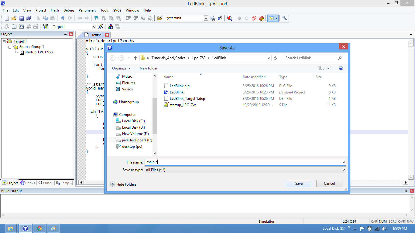
Step8: After typing the code save the file as main.c.
Step9: Add the recently saved file to the project.
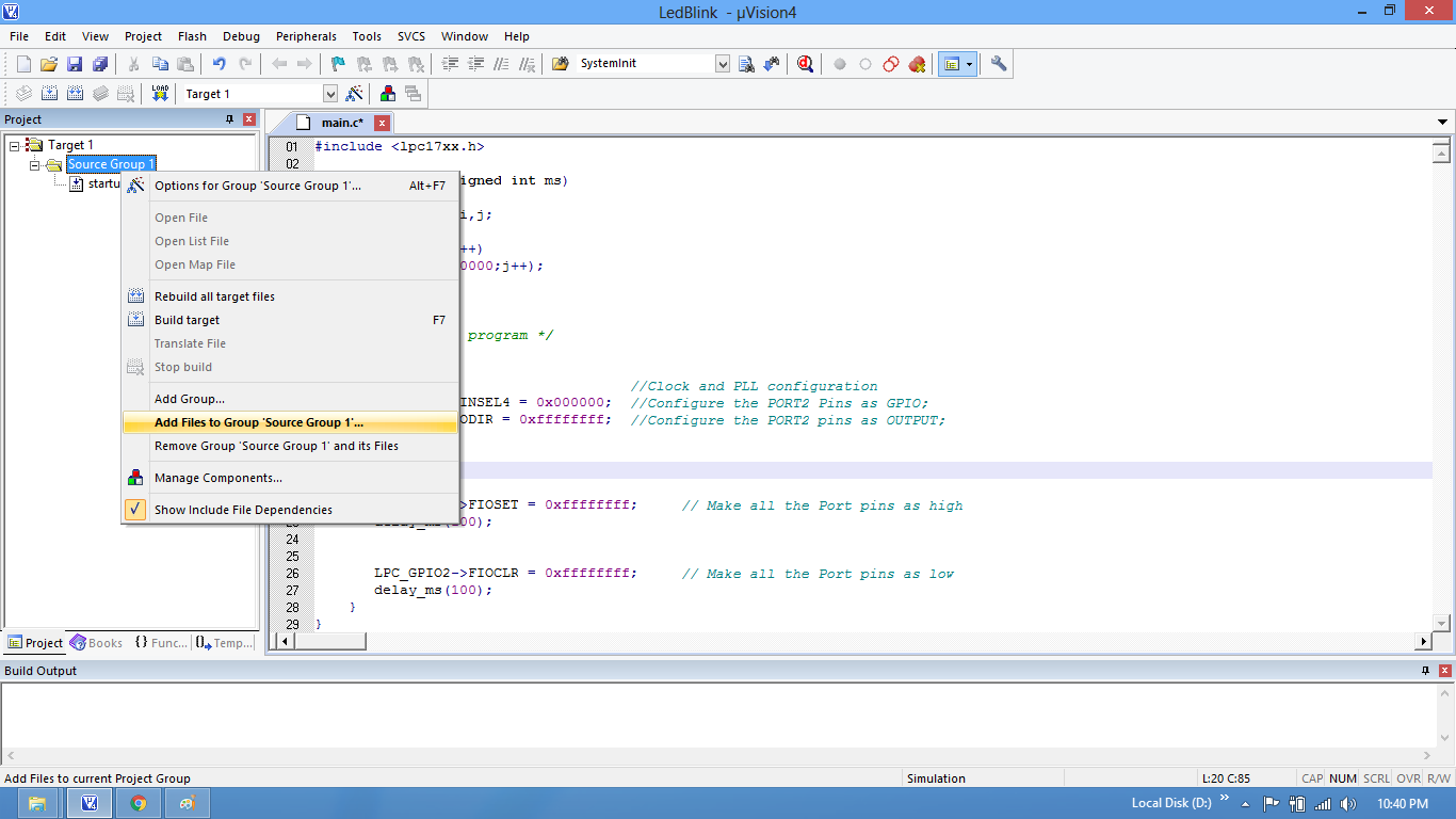
Step10: Add the main.c along with system_LPC17xx.c.
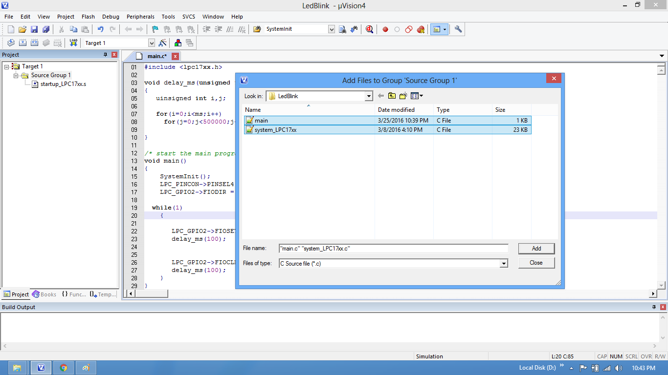
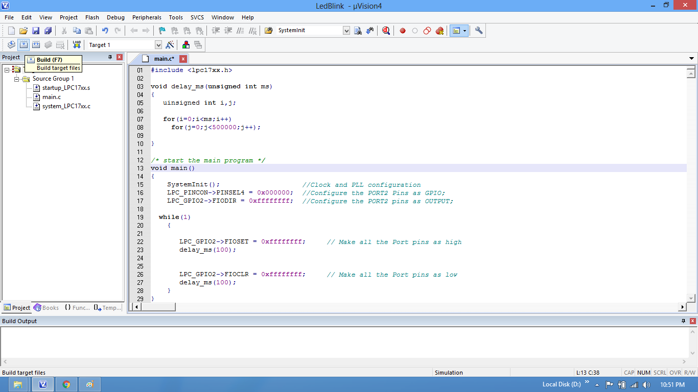
Step11: Build the project and fix the compiler errors/warnings if any.
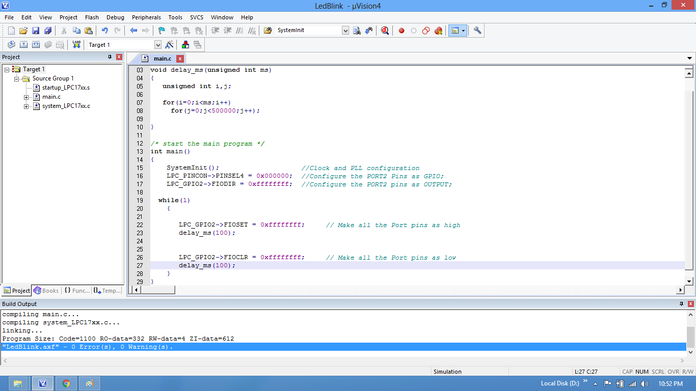
Step12: Code is compiled with no errors. The .bin file is still not generated.
Setup Bin File Generation
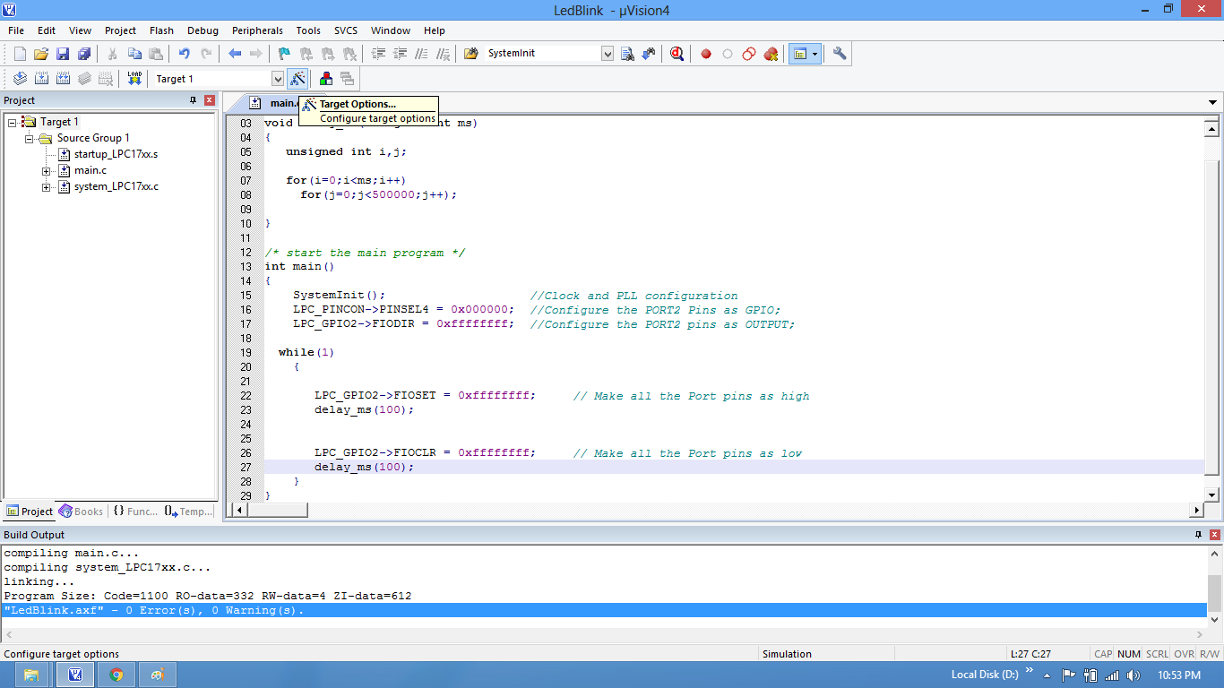
Step13: Click on Target Options to select the option for generating .bin file.
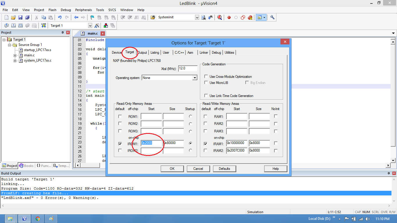
Step14: Set IROM1 start address as 0x2000. Bootloader will be stored from 0x0000-0x2000 so application should start from 0x2000
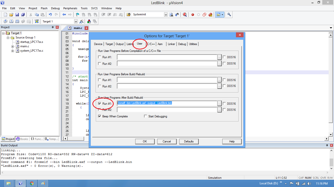
Step15: Write the command to generate the .bin file from .axf file
Command: fromelf --bin LedBlink.axf --output LedBlink.bin
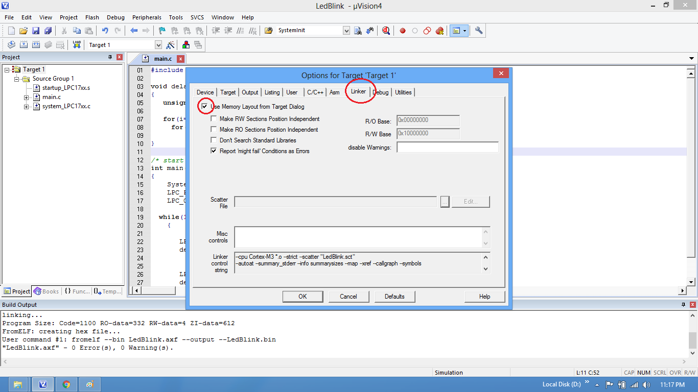
Step16: Now enable the linker option to use the IROM1 address from target settings
Step17: .Bin file is generated after a rebuild.
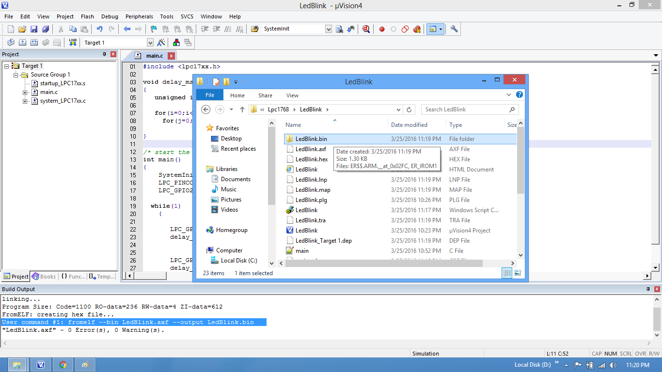
Step18: Check the project folder for the generated .Bin<ER_ROM1> file.
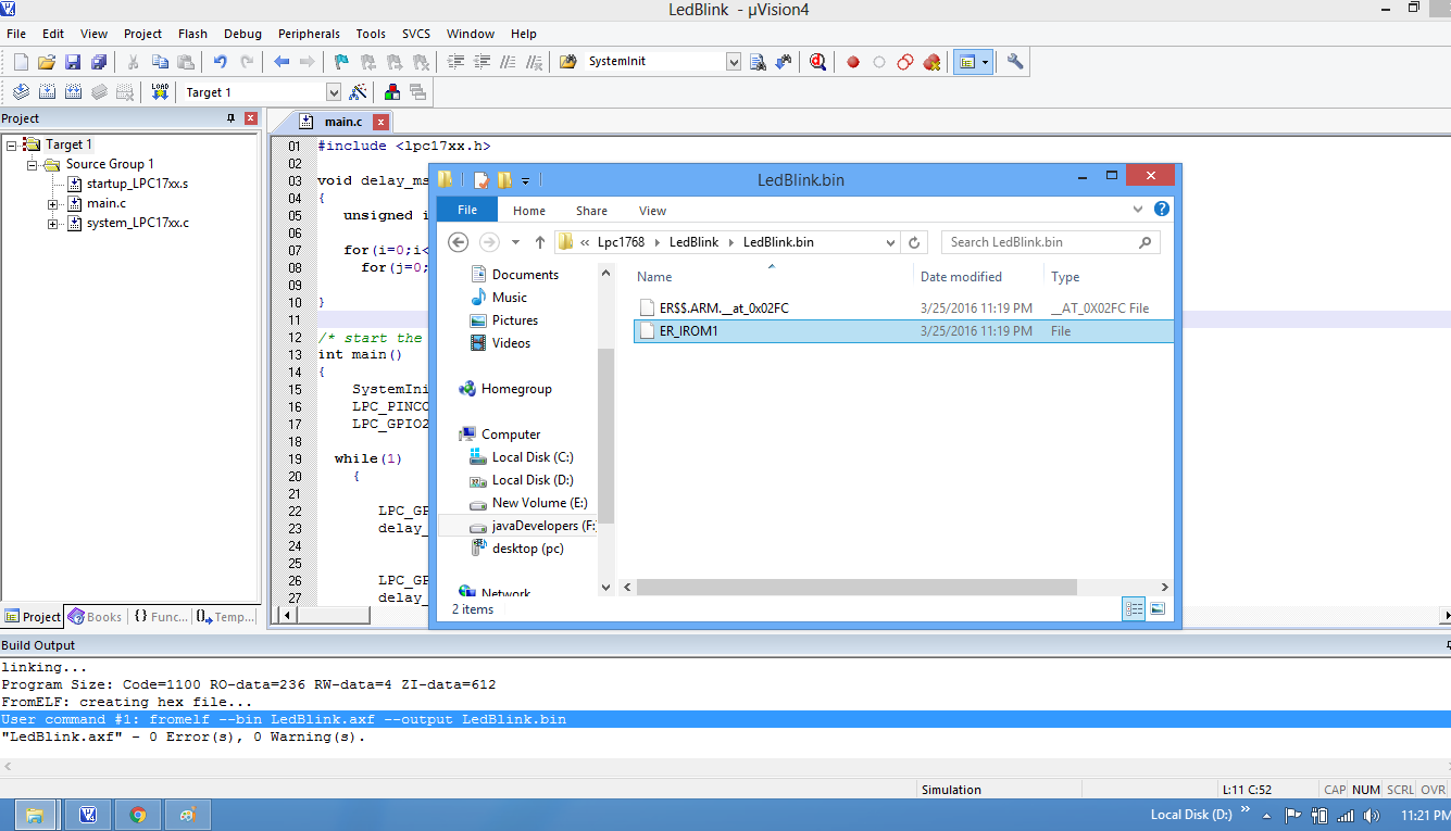
Uploading the Bin file
After generating the .bin file check this tutorial for Uploading Hex and Bin files..
Downloads
Download the complete project folder from the below link:
https://codeload.github.com/ExploreEmbedded/Explore-Cortex-M3-LPC1768-Stick-DVB-14001/zip/master
Have a opinion, suggestion , question or feedback about the article let it out here!