Difference between revisions of "ALU in Detail"
| (10 intermediate revisions by the same user not shown) | |||
| Line 1: | Line 1: | ||
{{box|type=green_dark|text=Arithmetic and Logic Unit in Detail}} | {{box|type=green_dark|text=Arithmetic and Logic Unit in Detail}} | ||
| − | {{box|type=l_green_light|text= You should have heard of an Arithmetic and Logic Unit before, while discussing a Computer CPU or a micro controller. In this tutorial we will look at what an ALU really is? <br /> | + | {{box|type=l_green_light|text=<br /> |
| + | =====Introduction===== | ||
| + | You should have heard of an Arithmetic and Logic Unit before, while discussing a Computer CPU or a micro controller. In this tutorial we will look at what an ALU really is? <br /> | ||
We will discuss a 4 bit ALU; this would limit many possibilities 16. We would assume that associated registers and instruction set are also 4 bit.<br /> | We will discuss a 4 bit ALU; this would limit many possibilities 16. We would assume that associated registers and instruction set are also 4 bit.<br /> | ||
| − | {| class="wikitable" style="text-align: | + | =====Half Adder ===== |
| + | Lets start with a simple half adder. | ||
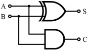
| + | '''Half adder''' adds two single binary digits ''A'' and ''B''. It has two outputs, sum (''S'') and carry (''C''). The carry signal represents an overflow into the next digit of a multi-digit addition.Figures below illustrate a simple half adder constructed from logic gates | ||
| + | }} | ||
| + | [[File:HalfAdder.png|right|thumb|Half adder logic diagram]] | ||
| + | {| class="wikitable" style="text-align:left" | ||
|- | |- | ||
!colspan="2"| Inputs !!colspan="2"| Outputs | !colspan="2"| Inputs !!colspan="2"| Outputs | ||
| Line 18: | Line 25: | ||
|} | |} | ||
| + | ===== Full Adder===== | ||
| + | {{box|type=l_green_light|text= | ||
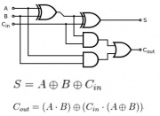
| + | ''Full Adder'' is an extension of half adder to include the Cin input as well. The truth table can be implemented to form the logic diagram as shown below. | ||
| + | }} | ||
| + | [[File:FullAdder.jpeg|thumbnail|Full Adder]] | ||
| − | == | + | {| class="wikitable" style="text-align:center" |
| + | |- | ||
| + | !colspan="3"| Inputs !!colspan="2"| Outputs | ||
| + | |- | ||
| + | ! ''A'' !! ''B'' !! ''C''<sub>in</sub> !! ''C''<sub>out</sub> !! ''S'' | ||
| + | |- | ||
| + | | 0 || 0 || 0 || 0 || 0 | ||
| + | |- | ||
| + | | 1 || 0 || 0 || 0 || 1 | ||
| + | |- | ||
| + | | 0 || 1 || 0 || 0 || 1 | ||
| + | |- | ||
| + | | 1 || 1 || 0 || 1 || 0 | ||
| + | |- | ||
| + | | 0 || 0 || 1 || 0 || 1 | ||
| + | |- | ||
| + | | 1 || 0 || 1 || 1 || 0 | ||
| + | |- | ||
| + | | 0 || 1 || 1 || 1 || 0 | ||
| + | |- | ||
| + | | 1 || 1 || 1 || 1 || 1 | ||
| + | |} | ||
| − | + | ===== The basic Unit: 1 bit ALU===== | |
| − | + | {{box|type=l_green_light|text= | |
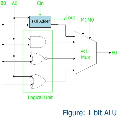
| + | So with the above building blocks, lets construct a simple ALU that performs a arithmetic operation (1 bit addition)and does 3 logical operations namely AND, NOR and XOR as shown below. The multiplexer selects only one operation at a time. | ||
| + | The operation selected depends on the selection lines of the multiplexer as shown in the truth table. | ||
| + | }} | ||
| + | [[File: 1bitALU.jpg|1000x480px|1 bit ALU]] | ||
| + | |||
| + | {| class="wikitable" style="text-align:left" | ||
| + | |- | ||
| + | !colspan="2"| Inputs !!colspan="2"| Outputs | ||
| + | |- | ||
| + | ! ''M1'' !! ''M0'' !! ''Operation'' | ||
| + | |- | ||
| + | | 0 || 0 || SUM | ||
| + | |- | ||
| + | | 1 || 0 || AND | ||
| + | |- | ||
| + | | 0 || 1 || OR | ||
| + | |- | ||
| + | | 1 || 1 || XOR | ||
| + | |- | ||
| + | |} | ||
| + | |||
| + | =====4 BIT ALU===== | ||
| + | {{box|type=l_green_light|text= | ||
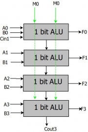
| + | Now we can take up the 1 bit ALU as block and construct a 4 bit ALU, which performs all the functions of the 1 bit ALU on the 4 bit inputs. | ||
| + | Thus a single building block can be constructed and used recursively. | ||
| + | The inputs A and B are four bits and the output is 4 bit as well. | ||
| + | Figure below illustrates it: | ||
}} | }} | ||
| + | [[File:4BITALU.jpg|frameless|4 bit ALU ]] | ||
| + | =====Important conclusions===== | ||
| + | {{box|type=l_green_light|text= | ||
| + | There are a few important takeaways here: | ||
| + | * The selection lines '''MO''' and '''M1''' select the function ALU performs. These selection lines combined with the input arguments and desired functions a '''''Instruction Set''''' can be formed. | ||
| + | * These Instructions can used to create meaningful programs. Since these are required to be easily available they can be stored on '''''ROM''''' unit. | ||
| + | * The input arguments '''A''' and '''B''' are often stored in '''Internal Registers'''. These along with other special purpose register form the '''registers''' of the microcontroller. | ||
| + | |||
| + | * ROM memories are slower in speed, hence an intermediate high speed ''RAM'' is often used. | ||
| + | *All the critical timings, decoding of the instructions are often grouped together in seperate '''''control and timings unit'''' | ||
| + | *If a Micro controller would be constructed only from ALU, RAM, ROM there would not be any external interface. Hence we have '''''Input/Output''''' IO ports. | ||
| + | *Additional features such as ''''''Interrupts, communication protocols, EEPROM, Timers/Counters, Debug interfaces etc ''''' are incorporated to make a controller complete. | ||
| + | |||
| + | In above discussion we might have left out intricate details involved in a ALU, CPU design. But the aim was to understand ALU/CPU at a deeper level. | ||
| + | |||
| + | }} | ||
| + | |||
| + | {{#widget:Facebook_Like_Box|profile=http://www.facebook.com/XploreLabz}} | ||
| + | |||
| + | {{DISQUS}} | ||
Latest revision as of 20:44, 28 September 2014
Contents
Introduction
You should have heard of an Arithmetic and Logic Unit before, while discussing a Computer CPU or a micro controller. In this tutorial we will look at what an ALU really is?
We will discuss a 4 bit ALU; this would limit many possibilities 16. We would assume that associated registers and instruction set are also 4 bit.
Half Adder
Lets start with a simple half adder. Half adder adds two single binary digits A and B. It has two outputs, sum (S) and carry (C). The carry signal represents an overflow into the next digit of a multi-digit addition.Figures below illustrate a simple half adder constructed from logic gates
| Inputs | Outputs | ||
|---|---|---|---|
| A | B | S | C |
| 0 | 0 | 0 | 0 |
| 1 | 0 | 1 | 0 |
| 0 | 1 | 1 | 0 |
| 1 | 1 | 0 | 1 |
Full Adder
| Inputs | Outputs | |||
|---|---|---|---|---|
| A | B | Cin | Cout | S |
| 0 | 0 | 0 | 0 | 0 |
| 1 | 0 | 0 | 0 | 1 |
| 0 | 1 | 0 | 0 | 1 |
| 1 | 1 | 0 | 1 | 0 |
| 0 | 0 | 1 | 0 | 1 |
| 1 | 0 | 1 | 1 | 0 |
| 0 | 1 | 1 | 1 | 0 |
| 1 | 1 | 1 | 1 | 1 |
The basic Unit: 1 bit ALU
| Inputs | Outputs | ||
|---|---|---|---|
| M1 | M0 | Operation | |
| 0 | 0 | SUM | |
| 1 | 0 | AND | |
| 0 | 1 | OR | |
| 1 | 1 | XOR | |
4 BIT ALU

Important conclusions
- The selection lines MO and M1 select the function ALU performs. These selection lines combined with the input arguments and desired functions a Instruction Set can be formed.
- These Instructions can used to create meaningful programs. Since these are required to be easily available they can be stored on ROM unit.
- The input arguments A and B are often stored in Internal Registers. These along with other special purpose register form the registers of the microcontroller.
- ROM memories are slower in speed, hence an intermediate high speed RAM is often used.
- All the critical timings, decoding of the instructions are often grouped together in seperate control and timings unit'
- If a Micro controller would be constructed only from ALU, RAM, ROM there would not be any external interface. Hence we have Input/Output IO ports.
- Additional features such as 'Interrupts, communication protocols, EEPROM, Timers/Counters, Debug interfaces etc are incorporated to make a controller complete.
In above discussion we might have left out intricate details involved in a ALU, CPU design. But the aim was to understand ALU/CPU at a deeper level.
{{#widget:Facebook_Like_Box|profile=http://www.facebook.com/XploreLabz}}


