Difference between revisions of "PCB DesignWorkshop"
| (25 intermediate revisions by 2 users not shown) | |||
| Line 1: | Line 1: | ||
{{box|type=blue_dark|text='''Workshop on PCB Design and Fabrication'''}} | {{box|type=blue_dark|text='''Workshop on PCB Design and Fabrication'''}} | ||
| + | [[category:Workshops]] | ||
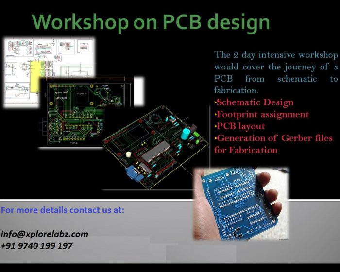
[[File:PCBTemplate.png|1080x560px]] | [[File:PCBTemplate.png|1080x560px]] | ||
| − | {{box|type= | + | ==Register for a Workshop== |
| + | {{box|type=l_green_light|text= | ||
| + | If you would like to attend any of our workshops, please fill up the '''[[Workshop_registration|workshop registration form.]]'''. | ||
| + | }} | ||
| + | =Workshop Contents= | ||
| + | {{box|type=l_green_light|text= | ||
The two day workshop would cover the following topics: | The two day workshop would cover the following topics: | ||
| − | ===Need for PCB.===<br | + | ======'''Need for PCB.'''====== |
| − | ===Introduction to KICAD.=== | + | Printed Circuit Boards are essential part of electronics; they provide a convenient way to rig up circuits and test them. Not only they ease prototyping they enhance reliability of the products. The bread boarding techniques do not quite work if the number of connects increase substantially. Hence even for Hobby users PCB design is becoming essential. Also with smaller packaging sizes for Integrated circuits it is almost impossible to prototype on Breadboard. PCB designing can be very joyful, and intricate. They say it is more of an art then science. Lots of scope for the designer. So Let's build a few of them.<br /> |
| − | ===A simple example: Schematic entry to PCB layout.=== | + | |
| − | ===Schematic Entry in detail:=== | + | ======'''Introduction to KICAD.'''====== |
| − | + | KiCAD is Open source and free software for schematic drawing, and PCB Layout. Commercial software of similar capability cost a good amount. It is not just about it, Open source allows more freedom, a rapid development and a chance to contribute to its development. We at [http://www.xplorelabz.com '''''Xplore Labz''''' ]use it for most of our designs. We strive to make user friendly tutorials on KiCAD. Check this [[A simple example for beginners: LED Breakout| '''''Basic Tutorial''''' ]] to get started. Workshops are extension of this endeavor to help you build hands ON!. | |
| − | + | ======'''A simple example: Schematic entry to PCB layout.'''====== | |
| − | + | In the first session of the workshop; we do a small PCB like a 4 led breakout, or a 555 timer etc, right from schematic to layout. This gives a complete flow on how to build a PCB with KiCAD. | |
| − | ===Generating Net list from schematic:=== | + | Following it we take up a advanced tutorial and do a hands on session with following topics in detail. |
| − | + | ======'''Schematic Entry in detail:'''====== | |
| − | + | *Creating custom components. | |
| − | ===Footprints:=== | + | *Importing standard libraries. |
| − | + | *Tools for creating components. | |
| − | + | ======'''Generating Net list from schematic:'''====== | |
| − | + | *Annotation schemes. | |
| − | + | *Matching schematic symbols to footprints. | |
| − | + | ======'''Footprints:'''====== | |
| − | + | *Component packages. | |
| − | ===Board layout:=== | + | *Measurement units & standards. |
| − | + | *Library footprints. | |
| − | + | *Importing footprints. | |
| − | + | *Creating custom footprints. | |
| − | + | *Tools for footprint generation. | |
| − | + | ======'''Board layout:'''====== | |
| − | + | *Importing Net list. | |
| − | + | *Footprint layout & form factor. | |
| − | + | *Layers of design. | |
| − | + | *Single layer, multilayer designs. | |
| − | + | *Manual routing | |
| − | ===Gerber file generation:=== | + | *Custom Tracks & vias. |
| − | + | *Track width calculation. | |
| − | + | *Auto Routing | |
| − | + | *Outline routing tools. | |
| − | ===PCB Fabrication:=== | + | *Generating custom routes. |
| − | + | ======'''Gerber file generation:'''====== | |
| − | + | *Finalizing the design. | |
| + | *Gerber file format for different layers. | ||
| + | *Appending multiple boards. | ||
| + | ======'''PCB Fabrication:'''====== | ||
| + | *Quick Presentation on PCB fabrication | ||
| + | *Checking FAB requirements. | ||
}} | }} | ||
| + | |||
| + | ==Sample Designs== | ||
| + | Here are a few sample designs which we do at our workshops, the list is not exhaustive, we do hands on designs at the workshops depending on the intended audience and their interest! Hover over the images to preview! | ||
| + | |||
| + | |||
| + | <gallery mode = "packed-hover"> | ||
| + | File:SevenSegment.PNG | ||
| + | File:MQSensor.PNG | ||
| + | File:Led_Array.PNG | ||
| + | File:Avr_mini_v1.PNG | ||
| + | File:AVR_ROBO.PNG | ||
| + | File:Bluetooth.PNG | ||
| + | File:Mega gsm.PNG | ||
| + | File:XploreUno.PNG | ||
| + | </gallery> | ||
| + | |||
| + | ==Video Tutorials== | ||
| + | It is not just the workshop, we continue our efforts to make high quality video tutorials. You can watch these tutorials later at home or office and improve your design skills. Our videos are listed on KiCADs Official website! | ||
| + | * 1. [[A simple example for beginners: LED Breakout|Basic Video for beginners.Cover the basics with a simple deisgn]] | ||
| + | * 2.[[ KiCAD: Advanced Tutorials:Arduino UNO with KiCAD|Advanced video series of 10 videos, covering a slightly complex PCB from schematic to gerbers! ]] | ||
| + | |||
| + | ==Downloads== | ||
| + | *[http://xplorelabz.com/wiki/images/6/6e/Xplore_UNO.zip Xplore_Uno Design Files] | ||
| + | *[http://xplorelabz.com/wiki/images/8/8d/Shields_and_Sensors.zip Sample Designs for Practice] | ||
| + | *[http://xplorelabz.com/wiki/images/e/e9/Presentation_on_PCB_Fabrication.pdf PCB Fabrication presentation] | ||
Latest revision as of 21:15, 14 December 2014
Contents
- 1 Register for a Workshop
- 2 Workshop Contents
- 2.1 Need for PCB.
- 2.2 Introduction to KICAD.
- 2.3 A simple example: Schematic entry to PCB layout.
- 2.4 Schematic Entry in detail:
- 2.5 Generating Net list from schematic:
- 2.6 Footprints:
- 2.7 Board layout:
- 2.8 Gerber file generation:
- 2.9 PCB Fabrication:
- 2.10 Sample Designs
- 2.11 Video Tutorials
- 2.12 Downloads
Register for a Workshop
Workshop Contents
Need for PCB.
Printed Circuit Boards are essential part of electronics; they provide a convenient way to rig up circuits and test them. Not only they ease prototyping they enhance reliability of the products. The bread boarding techniques do not quite work if the number of connects increase substantially. Hence even for Hobby users PCB design is becoming essential. Also with smaller packaging sizes for Integrated circuits it is almost impossible to prototype on Breadboard. PCB designing can be very joyful, and intricate. They say it is more of an art then science. Lots of scope for the designer. So Let's build a few of them.
Introduction to KICAD.
KiCAD is Open source and free software for schematic drawing, and PCB Layout. Commercial software of similar capability cost a good amount. It is not just about it, Open source allows more freedom, a rapid development and a chance to contribute to its development. We at Xplore Labz use it for most of our designs. We strive to make user friendly tutorials on KiCAD. Check this Basic Tutorial to get started. Workshops are extension of this endeavor to help you build hands ON!.
A simple example: Schematic entry to PCB layout.
In the first session of the workshop; we do a small PCB like a 4 led breakout, or a 555 timer etc, right from schematic to layout. This gives a complete flow on how to build a PCB with KiCAD. Following it we take up a advanced tutorial and do a hands on session with following topics in detail.
Schematic Entry in detail:
- Creating custom components.
- Importing standard libraries.
- Tools for creating components.
Generating Net list from schematic:
- Annotation schemes.
- Matching schematic symbols to footprints.
Footprints:
- Component packages.
- Measurement units & standards.
- Library footprints.
- Importing footprints.
- Creating custom footprints.
- Tools for footprint generation.
Board layout:
- Importing Net list.
- Footprint layout & form factor.
- Layers of design.
- Single layer, multilayer designs.
- Manual routing
- Custom Tracks & vias.
- Track width calculation.
- Auto Routing
- Outline routing tools.
- Generating custom routes.
Gerber file generation:
- Finalizing the design.
- Gerber file format for different layers.
- Appending multiple boards.
PCB Fabrication:
- Quick Presentation on PCB fabrication
- Checking FAB requirements.
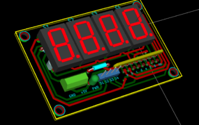
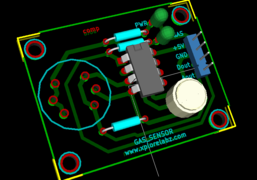
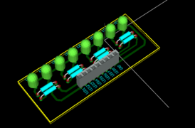
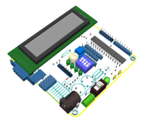
Sample Designs
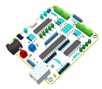
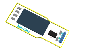
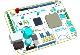
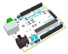
Here are a few sample designs which we do at our workshops, the list is not exhaustive, we do hands on designs at the workshops depending on the intended audience and their interest! Hover over the images to preview!
Video Tutorials
It is not just the workshop, we continue our efforts to make high quality video tutorials. You can watch these tutorials later at home or office and improve your design skills. Our videos are listed on KiCADs Official website!
- 1. Basic Video for beginners.Cover the basics with a simple deisgn
- 2.Advanced video series of 10 videos, covering a slightly complex PCB from schematic to gerbers!

