Difference between revisions of "Interfacing GLCD(128x64) with PIC16F877A"
| Line 60: | Line 60: | ||
[[FILE:GLCD Pages.png]] | [[FILE:GLCD Pages.png]] | ||
Lets view the GLCD as a open book with 2pages constisting of 8lines on each page.<br> | Lets view the GLCD as a open book with 2pages constisting of 8lines on each page.<br> | ||
| − | Each line has 64 cursors positions to data/images.<br> | + | Each line has 64 cursors positions to display data/images.<br> |
The required page can be selected using CS1,CS2 pins as shown below. | The required page can be selected using CS1,CS2 pins as shown below. | ||
<b>CS2-CS1:</b>Chip Select Lines<br> | <b>CS2-CS1:</b>Chip Select Lines<br> | ||
Revision as of 17:40, 20 May 2016
In this tutorial we will see how to interface and graphical LCD(GLCD) with PIC16F877A. In this tutorial we will look at interfacing KS0108 controller based JHD12864E display. There are many displays out there based on KS0108 or compatible display controller. They all work the same way, but make sure to check the datasheet for the pin diagram before doing the connection.
We will look at the working of the display, the hardware setup and programming with PIC16F877A. You may use any other AVR,8051,PIC,ARM controller as well. We have it tested and working on 8051, AVR, PIC and ARM. We have similar tutorials on these MCUs as well.
Unlike a 16 x 2 display, this does not have a character map for ascii values stored on its ROM. However it allows us the flexibility of creating fonts like Arial, times new roman etc. We could also display bit-map images on it and stretching it little further we can make GUI's and little animation, but that's for another day. So lets get started.
Contents
GLCD Internals And Pinout
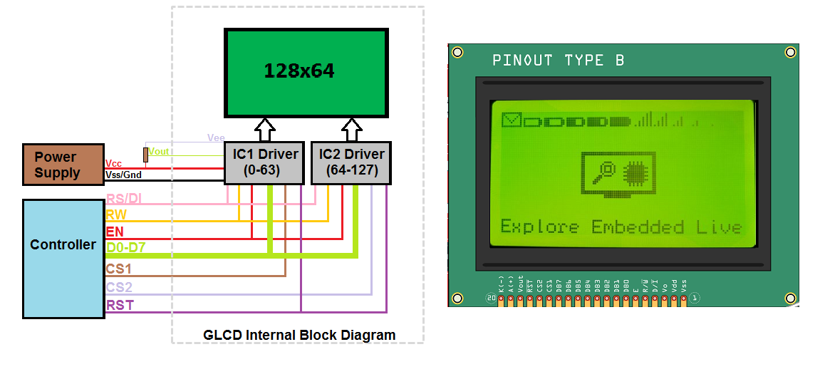
Below image shows the internal block diagram of 128x64 GLCD along with its pin out.
 As per the name it has 128pixels on X-axis and 64-pixels on Y-axis. Further the X-axis is divided into two parts of 64 pixels each and controlled by unique contoller/driver IC as shown in the above image.
Below table provides the detailed info of all the GLCD pins.
| Pin Number | Symbol | Pin Function |
| 1 | VSS | Ground |
| 2 | VCC | +5v |
| 3 | VO | Contrast adjustment (VO) |
| 4 | RS/DI | Register Select/Data Instruction. 0:Instruction, 1: Data |
| 5 | R/W | Read/Write, R/W=0: Write & R/W=1: Read |
| 6 | EN | Enable. Falling edge triggered |
| 7 | D0 | Data Bit 0 |
| 8 | D1 | Data Bit 1 |
| 9 | D2 | Data Bit 2 |
| 10 | D3 | Data Bit 3 |
| 11 | D4 | Data Bit 4 |
| 12 | D5 | Data Bit 5 |
| 13 | D6 | Data Bit 6 |
| 14 | D7 | Data Bit 7/Busy Flag |
| 15 | CS1 | Chip Select for IC1/PAGE0 |
| 16 | CS2 | Chip Select for IC2/PAGE1 |
| 17 | RST | Reset the LCD module |
| 18 | VEE | Negative voltage used along with Vcc for brightness control |
| 15 | A/LED+ | Back-light Anode(+) |
| 16 | K/LED- | Back-Light Cathode(-) |
Page and Line Selection
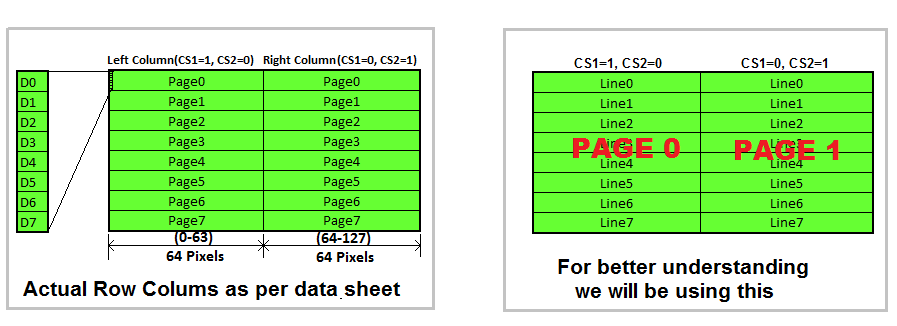
 Lets view the GLCD as a open book with 2pages constisting of 8lines on each page.
Each line has 64 cursors positions to display data/images.
The required page can be selected using CS1,CS2 pins as shown below.
CS2-CS1:Chip Select Lines
00 = Both Pages
01 = Page 0
10 = Page 1
11 = None
Line Selection
To select the lines we need to send the command/line address to GLCD.
The line address starts from 0xb8 and goes till 0xbf as shown below.
| 7 | 6 | 5 | 4 | 3 | 2 | 1 | 0 |
| 1 | 0 | 1 | 1 | 1 | Y3 | Y1 | Y0 |
Y2-Y0:Line Selection
000 = Line0 (Address = 0xB8)
001 = Line1 (Address = 0xB9)
010 = Line2 (Address = 0xBA)
011 = Line3 (Address = 0xBB)
100 = Line4 (Address = 0xBC)
101 = Line5 (Address = 0xBD)
110 = Line6 (Address = 0xBE)
111 = Line7 (Address = 0xBF)
Cursor/Char Position
To set the cursor position(0-63) we need to send its address to GLCD.
The cursor positions address starts from 0x40 and goes till 0x7f as shown below.
| 7 | 6 | 5 | 4 | 3 | 2 | 1 | 0 |
| 0 | 1 | x5 | x4 | x3 | x2 | x1 | x0 |
x5-x0:Line Selection
000000 = Cursor Position 0 (Address = 0x40)
000001 = Cursor Position 1 (Address = 0x41)
000002 = Cursor Position 2 (Address = 0x42)
111111 = Cursor Position 63 (Address = 0x7F)
