Difference between revisions of "PCB DesignWorkshop"
(a) |
|||
| Line 3: | Line 3: | ||
{{box|type=blue_light|text= | {{box|type=blue_light|text= | ||
The two day workshop would cover the following topics:<br\> | The two day workshop would cover the following topics:<br\> | ||
| − | ====='''Need for PCB.'''===== | + | ======'''Need for PCB.'''====== |
| − | ====='''Introduction to KICAD.'''===== | + | Printed Circuit Boards are essential part of electronics; they provide a convenient way to rig up circuits and test them. Not only they ease prototyping they enhance reliability of the products. The bread boarding techniques do not quite work if the number of connects increase substantially. Hence even for Hobby users PCB design is becoming essential. Also with smaller packaging sizes for Integrated circuits it is almost impossible to prototype on Breadboard. PCB designing can be very joyful, and intricate. They say it is more of an art then science. Lots of scope for the designer. So Let's build a few of them. |
| − | ====='''A simple example: Schematic entry to PCB layout.'''===== | + | ======'''Introduction to KICAD.'''====== |
| − | ====='''Schematic Entry in detail:'''===== | + | ======'''A simple example: Schematic entry to PCB layout.'''====== |
| + | ======'''Schematic Entry in detail:'''====== | ||
**Creating custom components. | **Creating custom components. | ||
**Importing standard libraries. | **Importing standard libraries. | ||
**Tools for creating components. | **Tools for creating components. | ||
| − | ====='''Generating Net list from schematic:'''===== | + | ======'''Generating Net list from schematic:'''====== |
**Annotation schemes. | **Annotation schemes. | ||
**Matching schematic symbols to footprints. | **Matching schematic symbols to footprints. | ||
| − | ====='''Footprints:'''===== | + | ======'''Footprints:'''====== |
**Component packages. | **Component packages. | ||
**Measurement units & standards. | **Measurement units & standards. | ||
| Line 20: | Line 21: | ||
**Creating custom footprints. | **Creating custom footprints. | ||
**Tools for footprint generation. | **Tools for footprint generation. | ||
| − | ====='''Board layout:'''===== | + | ======'''Board layout:'''====== |
**Importing Net list. | **Importing Net list. | ||
**Footprint layout & form factor. | **Footprint layout & form factor. | ||
| Line 31: | Line 32: | ||
**Outline routing tools. | **Outline routing tools. | ||
**Generating custom routes. | **Generating custom routes. | ||
| − | ====='''Gerber file generation:'''===== | + | ======'''Gerber file generation:'''====== |
**Finalizing the design. | **Finalizing the design. | ||
**Gerber file format for different layers. | **Gerber file format for different layers. | ||
**Appending multiple boards. | **Appending multiple boards. | ||
| − | ====='''PCB Fabrication:'''===== | + | ======'''PCB Fabrication:'''====== |
**Quick Presentation on PCB fabrication | **Quick Presentation on PCB fabrication | ||
**Checking FAB requirements. | **Checking FAB requirements. | ||
}} | }} | ||
Revision as of 14:06, 6 December 2013
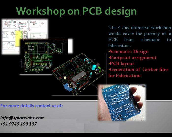
Workshop on PCB Design and Fabrication

The two day workshop would cover the following topics:<br\>
Contents
Need for PCB.
Printed Circuit Boards are essential part of electronics; they provide a convenient way to rig up circuits and test them. Not only they ease prototyping they enhance reliability of the products. The bread boarding techniques do not quite work if the number of connects increase substantially. Hence even for Hobby users PCB design is becoming essential. Also with smaller packaging sizes for Integrated circuits it is almost impossible to prototype on Breadboard. PCB designing can be very joyful, and intricate. They say it is more of an art then science. Lots of scope for the designer. So Let's build a few of them.
Introduction to KICAD.
A simple example: Schematic entry to PCB layout.
Schematic Entry in detail:
- Creating custom components.
- Importing standard libraries.
- Tools for creating components.
Generating Net list from schematic:
- Annotation schemes.
- Matching schematic symbols to footprints.
Footprints:
- Component packages.
- Measurement units & standards.
- Library footprints.
- Importing footprints.
- Creating custom footprints.
- Tools for footprint generation.
Board layout:
- Importing Net list.
- Footprint layout & form factor.
- Layers of design.
- Single layer, multilayer designs.
- Manual routing
- Custom Tracks & vias.
- Track width calculation.
- Auto Routing
- Outline routing tools.
- Generating custom routes.
Gerber file generation:
- Finalizing the design.
- Gerber file format for different layers.
- Appending multiple boards.
PCB Fabrication:
- Quick Presentation on PCB fabrication
- Checking FAB requirements.
