Difference between revisions of "Pic18f4520 Starter Board Introduction"
| Line 32: | Line 32: | ||
This Board will comes with Two on board LEDs Connected to PD0 and PD1. | This Board will comes with Two on board LEDs Connected to PD0 and PD1. | ||
[[File:PIC18f4520 LED.png]]<br><br> | [[File:PIC18f4520 LED.png]]<br><br> | ||
| − | |||
| − | |||
===LCD Test=== | ===LCD Test=== | ||
Below table shows the LCD 4-bit pin connection. | Below table shows the LCD 4-bit pin connection. | ||
| Line 40: | Line 38: | ||
!RS || RW || EN || D4 || D5 || D6 || D7 | !RS || RW || EN || D4 || D5 || D6 || D7 | ||
|- | |- | ||
| − | |PB_0 || PB_1 || PB_2 || | + | |PB_0 || PB_1 || PB_2 || PB_4 || PB_5 || PB_6 || PB_7 |
|} | |} | ||
<br> | <br> | ||
[[File:PIC18f4520 LCD.png]]<br><br> | [[File:PIC18f4520 LCD.png]]<br><br> | ||
| − | |||
===Switch Test=== | ===Switch Test=== | ||
The Board comes with two on Board Switches, Connected to PD2 and PD3. | The Board comes with two on Board Switches, Connected to PD2 and PD3. | ||
[[File:PIC18f4520 Switch.png]]<br><br> | [[File:PIC18f4520 Switch.png]]<br><br> | ||
| − | |||
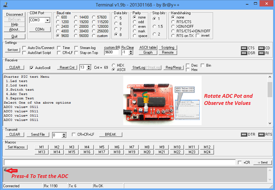
===Adc Test=== | ===Adc Test=== | ||
The Board has a Pot Connected to AN0/RA0. ADC values from the Pot is read and transmtted on UART. | The Board has a Pot Connected to AN0/RA0. ADC values from the Pot is read and transmtted on UART. | ||
[[File:PIC18f4520 ADC.png]]<br><br> | [[File:PIC18f4520 ADC.png]]<br><br> | ||
| − | |||
| − | |||
| − | |||
| − | |||
===EEprom Test=== | ===EEprom Test=== | ||
(A-Z) is wriiten to eeprom and then read it back. Same is transmitted on UART. | (A-Z) is wriiten to eeprom and then read it back. Same is transmitted on UART. | ||
[[File:PIC18f4520 EEPROM.png]]<br><br> | [[File:PIC18f4520 EEPROM.png]]<br><br> | ||
Revision as of 17:04, 9 August 2016
Kit Contents: PIC18F4520 Starter Board comes with the following features:
- PIC18F4520 MCU with ds30 bootloader
- LCD 16x2 breakout.
- On Board Usb-To-Serial.
- Test switches (2) and LEDs(2).
- All Port pins available for peripheral interfacing.
- Dimensions: 90mm X 70mm.
- 1.6mm Glass Epoxy, FR4 PCB.
- Wave Soldered.
Contents
Driver Installation
- Check this tutorial for Usb2Serial Driver Installation.
Software Setup
- Compiler Installation: Download and Install the MPlabx IDE and x8 compiler.
- Check this tutorial for setting up the project to generate the .hex file.
- Check this tutorial for Uploading Hex File Using Pickit2.
- Check this tutorial for Uploading Hex File Using Ds30 Bootloader.
Complete Board Test
The board is shipped with test software loaded in the controller. Connect the board to the System, Open the Serial Terminal and reset the Controller. Follow the below procedure to test all the peripherals.
GPIO Test
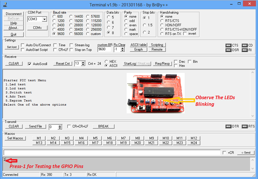
This Board will comes with Two on board LEDs Connected to PD0 and PD1.
LCD Test
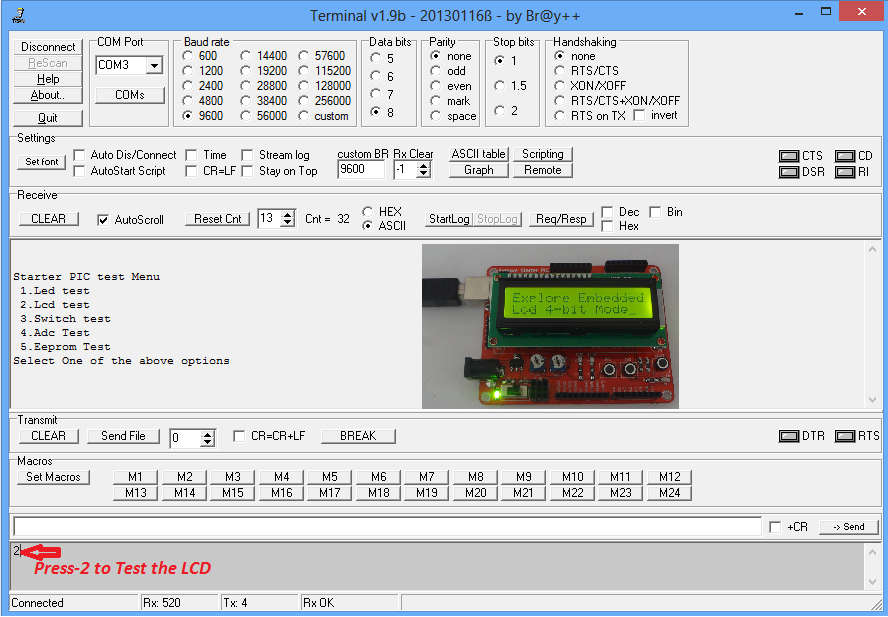
Below table shows the LCD 4-bit pin connection.
| RS | RW | EN | D4 | D5 | D6 | D7 |
|---|---|---|---|---|---|---|
| PB_0 | PB_1 | PB_2 | PB_4 | PB_5 | PB_6 | PB_7 |
Switch Test
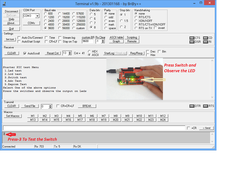
The Board comes with two on Board Switches, Connected to PD2 and PD3.
Adc Test
The Board has a Pot Connected to AN0/RA0. ADC values from the Pot is read and transmtted on UART.
EEprom Test
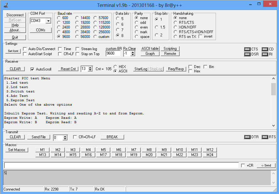
(A-Z) is wriiten to eeprom and then read it back. Same is transmitted on UART.
