OLED Interface With 8051
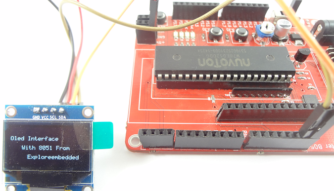
In earlier tutorials, we discussed the interfacing of LCD and GLCD. In this tutorial, we will see how to interfaces an I2C OLED(128x64) with 8051. There are plenty of well written arduino oled libraries(AdaFruit SSD1306, rinkydinkelectronics) for displaying strings, numbers, and logos. They all use a shadow ram buffer of 1024 bytes(128x64 pixels) and support different fonts and graphics. As 8051 has only 128 bytes of RAM we cannot use the shadow RAM buffer and cannot support all the fonts and graphics.
First, we will see the frame format for sending the commands and data to OLED. After this, we will discuss few of the OLED commands. Finally, we will be displaying string, numbers on OLED.
Displaying of logos/icons will be discussed in the separate tutorial.

OLED Frame Format
The OLED I2C communication interface consists of slave address bit SA0, I2C-bus data signal SDA and I2C-bus clock signal SCL. Both the data and clock signals must be connected to pull-up resistors.
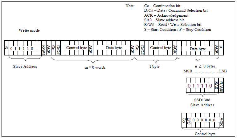
- Slave address bit (SA0): As the I2c communication depends on the slave address(ID) and will respond only if it matches. SSD1306 OLED device will respond to the slave address following the slave address bit (“SA0” bit) and the read/write select bit (“R/W#” bit) with the following byte format,
| B7 | B6 | B5 | B4 | B3 | B2 | B1 | B0 |
|---|---|---|---|---|---|---|---|
| 0 | 1 | 1 | 1 | 1 | 0 | SA0 | R/W |
SA0 bit provides an extension bit for the slave address. Either “0111100” or “0111101”, can be selected as the slave address of SSD1306.
R/W bit is used to determine the operation mode of the I2C-bus interface.
R/W=1, it is in read mode.
R/W=0, it is in write mode.
- I2C-bus data signal (SDA): SDA pin is used to send or receive the information between the master and slave. This will also be used for sending the acknowledgement.
- I2C-bus clock signal (SCL): The transmission of information in the I2C-bus is controlled by clock signal(SCL). One bit of information is transmitted/received during a single clock period of SCL.
The I2C-bus interface gives access to write data and command into the device. Below image shows the write mode of I2C-bus in chronological order.

- The master device initiates the data communication by a start condition. The start condition is established by pulling the SDA from HIGH to LOW while the SCL stays HIGH.
- The slave address is sent immediately after the Start Condition. For the SSD1306, the slave address is either “b0111100” or “b0111101” by changing the SA0 to LOW or HIGH (D/C pin acts as SA0).
- The write mode is established by setting the R/W bit to logic “0”.
- An acknowledgement signal will be generated after receiving one byte of data, including the slave address and the R/W bit.The acknowledge bit is defined as the SDA line is pulled down during the HIGH period of the acknowledgement related clock pulse.
- After the transmission of the slave address, either the control byte or the data byte may be sent across the SDA. A control byte mainly consists of Co and D/C# bits following by six “0” ‘s. If the Co bit is set as logic “0”, the transmission of the following information will contain data bytes only. The D/C bit determines the next data byte is acted as a command or a data. If the D/C bit is set to logic “0”, it defines the following data byte as a command. If the D/C bit is set to logic “1”, it defines the following data byte as a data which will be stored at the GDDRAM. The GDDRAM column address pointer will be increased by one automatically after each data write.
- Acknowledge bit will be generated after receiving each control byte or data byte.
- The write mode will be finished when a stop condition is applied. The stop condition is established by pulling the “SDA in” from LOW to HIGH while the “SCL” stays HIGH.
OLED Commands
| Command | Command | Description |
|---|---|---|
| 0x00 | SSD1306_COMMAND | This command is used to indicate the next data byte is acted as a command. |
| 0x40 | SSD1306_DATA_CONTINUE | This command sets the Display Start Line register to determine starting address of display RAM |
| 0xAE | SSD1306_DISPLAY_OFF | This command is used to turn OFF the OLED display panel. |
| 0xAF | SSD1306_DISPLAY_ON | This command is used to turn ON the OLED display panel. |
| 0x20 | SSD1306_MEMORY_ADDR_MODE | If horizontal address increment mode is enabled by command 20h, after finishing read/write one column data, it is incremented automatically to the next column address. |
| 0x21 | SSD1306_SET_COLUMN_ADDR | This command is used to define the current read/write column address in graphic display data RAM. |
| 0x22 | SSD1306_SET_PAGE_ADDR | This command is used to define the current read/write Line(Page as per data sheet) address in graphic display data RAM. |
| 0x81 | SSD1306_SET_CONTRAST_CONTROL | This command sets the Contrast Setting of the display. The chip has 256 contrast steps from 00h to FFh. The segment output current increases as the contrast step value increases. |
| 0xA6 | SSD1306_NORMAL_DISPLAY | This command sets the display to normal mode. In normal display a RAM data of 1 indicates an “ON” pixel. |
| 0xA7 | SSD1306_INVERT_DISPLAY | This command sets the display to inverse mode. In normal display a RAM data of 0 indicates an “ON” pixel. |
Command Write
Oled Init
Below Command needs to send to OLED for initialization:
- Display is OFF
- 128 x 64 Display Mode
- Normal segment and display data column address and row address mapping (SEG0 mapped to address 00h and COM0 mapped to address 00h)
- Shift register data clear in serial interface
- Display start line is set at display RAM address 0
- Column address counter is set at 0
- Normal scan direction of the COM outputs
- Contrast control register is set at 7Fh
- Normal display mode (Equivalent to A4h command)
Example Code
Below is sample code to display the Strings at different cursor positions.

Downloads
Download the sample code and design files from this link.
Have an opinion, suggestion , question or feedback about the article let it out here!
