Explore LPC2148 Board
In this tutorial, we will be discussing the features of the LPC2148 controller and Explore LPC2148 board. Once we have the fair idea of the board and its features we will look into the software/tool setup(Keil, Flash magic, Serial terminal etc). Once everything is ready we will test all the peripherals using a single test software.
The ARM LPC2148 chip has been out for quite some time now. This could be your first foray into the world of ARM microcontrollers. There are lots of resources and tools out there for this microcontroller. Hence we decided to make it into Explore Stick form factor.The board also has a USB bootloader which making programming the microcontroller extremely use. You simply need to drag and drop the bin file. The board breaks out most of the pins and it fits on a breadboard!.
Note : Debugger doesn't work with this board.
LPC2148 core features:
- Runs at 60Mhz(with PLL enabled)
- 512K Bytes Flash
- 32K Bytes RAM
- USB 2.0 Full-speed compliant device controller with 2 kB of endpoint RAM. In addition, the LPC2146/48 provides 8 kB of on-chip RAM accessible to USB by DMA.
- Two 10-bit ADCs provide a total of 6/14 analog inputs, with conversion times as low as 2.44 µs per channel.
- Single 10-bit DAC provides variable analog output (LPC2142/44/46/48 only).
- Two 32-bit timers/external event counters (with four capture and four compare channels each), PWM unit (six outputs) and watchdog.
- Low power Real-Time Clock (RTC) with independent power and 32 kHz clock input.
- Multiple serial interfaces including two UARTs (16C550), two Fast I²C-bus (400 kbit/s), SPI and SSP with buffering and variable data length capabilities.
- Vectored Interrupt Controller (VIC) with configurable priorities and vector addresses.
- Up to 45 of 5 V tolerant fast general-purpose I/O pins in a tiny LQFP64 package.
- Up to 21 external interrupt pins available.
- 60 MHz maximum CPU clock available from programmable on-chip PLL with settling time of 100 µs.
- On-chip integrated oscillator operates with an external crystal from 1 MHz to 25 MHz.
- Power saving modes include Idle and Power-down.
- Individual enable/disable of peripheral functions as well as peripheral clock scaling for additional power optimization.
- Processor wake-up from Power-down mode via external interrupt or BOD.
- Single power supply chip with POR and BOD circuits:
- CPU operating voltage range of 3.0 V to 3.6 V (3.3 V ± 10 %) with 5 V tolerant I/O pads
Board Features:
- USB bootloader- No external programmer required
- Onboard RTC battery support
- User LEDs x 4
- Switches x 4
- Note: Debugger doesn't work with this board.
Tool Setups
- Check this tutorial LPC2148 Keil Setup for generating the .bin file using keil.
Uploading Bin File
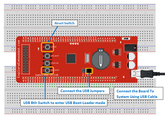
This board comes with secondary(USB) boot-loader with which you can just drag and drop the .bin file.
Follow the below steps to upload the new .bin file to LPC1768 board:
- Connect the USB Jumpers.
- Connect the ExploreLpc2148 to the system using a USB cable.
- Hold the USB_Btlr switch.
- Press the Reset Switch.
- Release the Reset Switch.
- Release the USB_Boot switch.
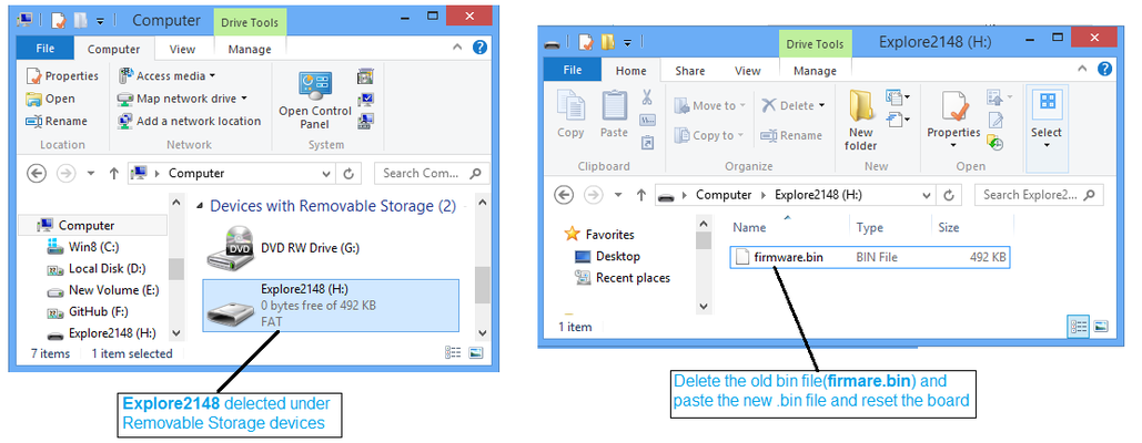
- Now the board will be detected as Explore2148 as shown in the second image.
- Delete the old firmware.bin file.
- Paste the new .bin file.
- Reset the Board.
- Now your Application code should be running on the board.
Have an opinion, suggestion , question or feedback about the article let it out here!


